Electron Beam Evaporation Coating (EB-PVD) Processes and Advantages and Disadvantages
Processes and Advantages of Electron Beam Evaporation Coating (EB-PVD) Electron Beam
Silicon nitride thin film windows are an important component of transmission electron microscopy (TEM) and scanning electron microscopy (SEM) analysis. Silicon nitride thin film windows are used in a variety of research applications such as semiconductor production and analysis, bioscience and materials science. Choosing the right silicon nitride thin film window for your research needs is critical to obtaining high quality data in TEM and SEM applications. In this article, we will discuss the key points to consider when selecting the right silicon nitride thin film window.
Chip frame size, film thickness, number of windows, window size, stress condition, cleanliness, flatness, coating
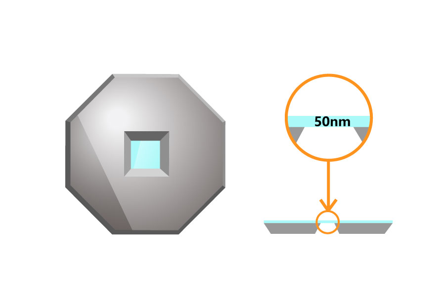
The frame size of the silicon nitride thin film window is usually chosen based on the size and shape of the sample holder (sample rod) to ensure that the window can be fixed to the sample rod and fit tightly with it to avoid sample movement or distortion.
The size and shape of the sample bar varies depending on the instrument model and the purpose of use. For microscopes such as transmission electron microscopy (TEM) and scanning electron microscopy (SEM), the sample bar is usually cylindrical and is available in different diameter and length options. Therefore, the frame size of the silicon nitride thin film window should match the diameter and length of the sample bar to ensure that it is securely fastened to the sample bar and provides sufficient support to protect the thin film window from mechanical stress. Other factors such as the thickness of the window material and the shape of the window should also be considered when choosing the frame size of the silicon nitride window. A conventional TEM silicon nitride thin film window has a chip frame size of 3 mm in diameter.
In addition, in actual use, it is necessary to select the appropriate window size and frame size according to the specific experimental needs and operation methods.
These 5 key points need to be considered in the selection of film thickness, imaging resolution, mechanical strength, ease of handling, andApplicationsand cost budget.
Key Points | Description |
|---|---|
Imaging resolution | For higher resolution, choose a thinner film, which is more transparent |
Mechanical strength | The thicker the film thickness the greater the mechanical strength. However, if the film thickness is too thick, it will lead to deterioration of optical properties and increase of manufacturing difficulty, therefore, a balance between film thickness and optical properties is needed. |
Ease of handling | Thicker films may be easier to handle and manipulate when preparing samples, while thinner films may require more delicate handling to avoid damage |
Applications | For example: In transmission electron microscopy (TEM), thinner films are preferred to maximize electron beam transmission and minimize image distortion. a common thickness for TEM grids is 20 nm, which provides good imaging clarity and contrast.
In scanning electron microscopy (SEM), thicker films may be preferred to improve mechanical stability and prevent film damage during imaging. Films between 50 nm and 100 nm thick are commonly used for SEM imaging. |
Cost Budget | It will be cheaper to use regular film thickness, and if special applications require thinner (e.g. 5nm, 8nm) or thicker (300nm, 500nm, etc.) then customization will be required and the cost will increase. (Harbor Semiconductor provides customization services) |
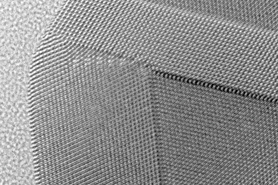
A thinner film can provide higher imaging resolution, but it may also be more fragile and easily damaged during sample preparation. On the other hand, thicker films are more robust, but may result in lower imaging resolution. 10 nm thickness is typically used for high-resolution imaging, while thicker films of 20-50 nm are typically used for general imaging and analysis.
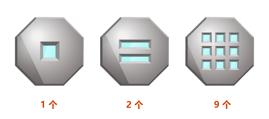
The number of windows in a silicon nitride thin film window should be determined based on specific experimental needs and sample type, with three considerations.
Key Points | Description |
|---|---|
Sample Type | Samples are relatively large or need to be observed in multiple areas, silicon nitride thin film windows with multiple windows can be selected to improve the efficiency and coverage of sample observation. |
Experimental requirements | When different experiments need to be performed or different samples need to be observed, silicon nitride film windows with multiple windows can be selected to facilitate quick sample changes or switching experiment types. |
Experimental equipment | The microscope or analysis equipment used that can only accommodate a single window of silicon nitride thin film window can only be selected for the number of windows in a single window. |
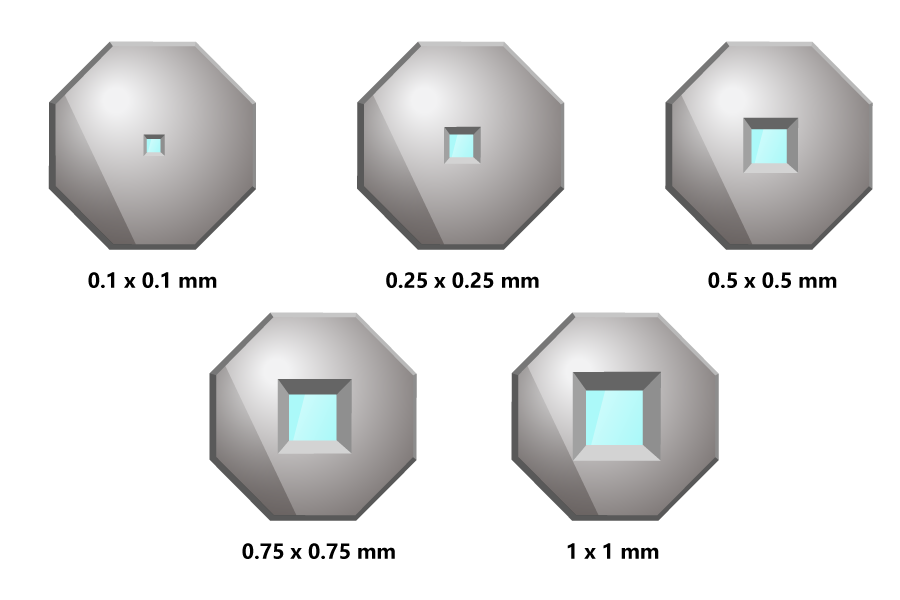
The window size determines the amount of electron flux that can pass through the window and reach the sample. Smaller window sizes can provide higher imaging resolution, but may also result in reduced signal intensity. For general imaging and analysis, larger window sizes are preferred, while for high-resolution imaging, smaller aperture sizes are recommended. Common window sizes used for TEM applications range from 0.1 mm to 1 mm.
Key Points | Description |
|---|---|
Sample characteristics | The appropriate window size is chosen according to the characteristics of the sample such as size, shape and surface structure. For larger samples or samples that need to be observed over a large area, a larger window is usually required to obtain a wider field of view; for samples with tiny or complex structures, a smaller window can be used to obtain higher resolution and better contrast. |
Optical Performance | The choice of window size also depends on the optical performance requirements. A smaller window improves resolution and contrast, but reduces optical transmittance. Larger windows can improve transmittance, but at the expense of resolution and contrast. |
Mechanical strength | The window size also affects the mechanical strength of the silicon nitride film window. In general, a smaller window size will improve the mechanical strength and stability of the film, but may limit the field of view and optical transmittance of the sample. Larger window sizes improve the field of view and optical transmittance of the sample, but may affect the mechanical strength and stability of the film. |
A rectangular window shape is also available. A rectangular silicon nitride film window provides a larger sample area, thus allowing larger samples to be placed under the window or a wider range of experiments to be performed on the sample surface. This is very beneficial for some experiments that require a large area for observation.
And it can also be adapted to the needs of experiments in different directions. For example, if the experiment needs to be performed in the horizontal direction, a wider rectangular window can be selected, while if the experiment needs to be performed in the vertical direction, a narrower rectangular window can be selected.
When selecting the stress case for the silicon nitride thin film window, factors such as the characteristics of the sample, the operating conditions of the microscope, and the purpose of the experiment need to be considered.
For example, in biological research, silicon nitride film windows with lower stresses need to be selected to avoid damage to the sample. While in materials science research, silicon nitride thin film windows with higher stresses need to be selected to obtain more accurate experimental results.
Cleanliness isSilicon nitride thin film windowsAnother key consideration. The purity and uniformity of the material can affect the quality of the data obtained during TEM and SEM analysis. Silicon nitride film windows made from high-purity materials are preferred to reduce contamination and ensure reproducible results. Harbor Semiconductor's silicon nitride films are coated by a dedicated silicon nitride furnace to minimize contamination. In addition, the use of materials with low background scattering, such as ultra-thin carbon films or pure silicon films, can also improve imaging quality.
The flatness of the silicon nitride film window has an effect on its imaging effect and experimental results in the microscope.
If the surface of the silicon nitride film window is not flat, it may lead to scattering and shifting during imaging, affecting the quality and resolution of the imaging.
Second, flatness also affects its positioning and stability in the microscope. If the silicon nitride film window is not flat, it may drift or jitter in the microscope, affecting the accuracy and reproducibility of the experiment.
In addition, the flatness of the silicon nitride film window affects its imaging depth and focusing performance in the microscope. If the surface of the silicon nitride film window is not flat, it may lead to changes in the imaging depth, making the imaging depth of different parts of the sample different. At the same time, the flatness of the silicon nitride film window also affects the focusing performance of the microscope, making it difficult to adjust the focal length during imaging.
Therefore, in order to obtain better imaging effects and experimental results, the flatness of the silicon nitride film window should be kept as good as possible, especially in high-resolution imaging or precision experiments. The flatness of the silicon nitride film window of Harbor Semiconductor is super high and very suitable for high-resolution imaging. At the same time, for experiments that require focusing or focussing, special attention needs to be paid to the flatness of the silicon nitride film window to ensure the clarity and accuracy of the imaging.
Silicon nitride thin film windows can be coated with various materials to improve their performance. such as enhancing their optical transmission or reducing their surface roughness. The choice of coating will depend on the specific application and the desired properties. For example, a thin layer of gold can be deposited on the surface of a silicon nitride window to increase its electrical conductivity and make it suitable for applications such as electrochemistry or impedance spectroscopy.
In summary, selecting the right silicon nitride film window for your research needs is key to ensuring accurate and reliable results. Factors such as thickness, size, coating, surface finish and chemical resistance should be carefully considered based on the specific requirements of your application. Consulting with the supplier or manufacturer (Harbor Semiconductor) and other researchers in your field can provide valuable insight and guidance in selecting the right window for your research needs.
We offer Silicon Nitride Thin Film Windows / MEMS Customization Services, Feel free to leave a message to inquire.
Processes and Advantages of Electron Beam Evaporation Coating (EB-PVD) Electron Beam
What are the properties and applications of silicon dioxide films prepared by electron beam evaporation? Dioxide
Principles and Applications of Optical Coating Technology The process principles of optical coating mainly involve
.jpg)