
In-depth science: introduction, types and applications of electron microscope carrier mesh (copper mesh)
Electron microscopy is an important tool for material analysis, which can observe the internal structure and composition of substances at the microscopic scale. And the electron microscope carrier mesh plays a crucial role as an important carrier for the preparation of samples for transmission electron microscopy. Therefore, understanding the basic concept, classification method and preparation process of transmission electron microscopy carrier mesh is important for the successful performance of transmission electron microscopy experiments and the accuracy of analytical data.
Basic concepts of electron microscope carrier network
It is a flat disk with a grid structure or other shaped holes. Its main function is to support and hold the sample during TEM observation, so that the sample remains stable while being observed in TEM.
Holes in the carrier mesh allow the electron beam to pass through the mesh, allowing the sample to be transmitted and observed by the electron beam. Depending on the needs of the sample to be observed, polymer and carbon films are loaded on the carrier mesh to make a carrier mesh (support film).
Types of electron microscope carrier networks
There are different classifications for transmission electron microscopy, including mesh shape and structure, mesh size, mesh material and special mesh.
Mesh shape structure
The shape structure of the pores of the carrier mesh has a great influence on the sample preparation and observation results. Round-hole bare mesh and square-hole bare mesh are two common hole shapes. Square-hole mesh has a more regular hole structure and smaller hole size, which can provide better preparation and observation results. In addition, the hole shape of the carrier mesh can be designed according to the actual needs, such as aperture, trapezoid and other irregular hole shapes of the carrier mesh.

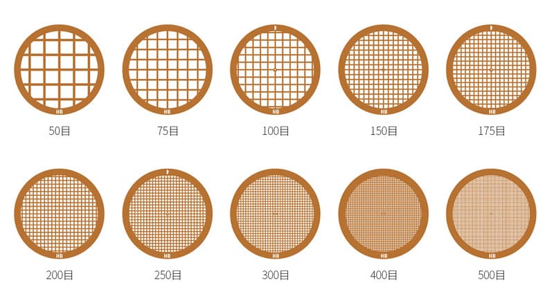
Mesh size
Mesh size refers to the size and number of mesh-carrying holes and has different effects on the preparation and observation of different samples. Smaller pore sizes can provide higher spatial resolution and better image detail, but can also limit the size and shape of the sample. It is generally classified into 50 mesh to 2000 mesh, and the aperture size can range from 800 μm to 6.5 μm. The commonly used mesh size is 100-200 mesh with proper hole size and spatial resolution, which can meet most of the transmission electron microscope sample preparation and observation requirements.
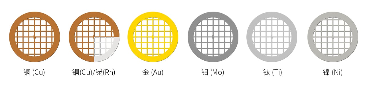
Carrier mesh material
The material of the carrier mesh has an important influence on the sample preparation and observation results. Different materials have different properties such as conductivity, strength and stability. For example, copper mesh is a commonly used carrier material with good electrical conductivity and strength, but under some specific experimental conditions, other materials such as nickel, molybdenum, gold, titanium, aluminum, etc. are also required.
The material of the carrier mesh has an important influence on the sample preparation and observation results. Different materials have different properties such as conductivity, strength and stability. For example, copper mesh is a commonly used carrier material with good electrical conductivity and strength, but under some specific experimental conditions, other materials such as nickel, molybdenum, gold, titanium, aluminum, etc. are also required.
Special Application Carrier Network
Stalked Network
A handled net is a net with a handle or grip. The handle can be used to manipulate and move the net. Handled nets are used in a wide variety of laboratory and manufacturing operations, especially in sample preparation and processing, to avoid contact with the net area.
Duplex Carrier Network
Duplex carrier screens, also known as folded carrier screens, are suitable for materials that do not easily adhere to the surface of conventional carrier screens and need to be sandwiched between two carrier screens and for large particle materials. It is ideal for holding thin metal foils in place. The mesh sizes of the two carriers can be different.
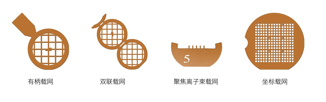
Focused Ion Beam Carrier Network (Lift Out Grids)
The focused ion beam is a TEM carrier network that receives milling by a FIB or SEM/FIB system.
Coordinate carrier network
A coordinate grid is a letter or number engraved on the carrier grid to mark the location of the sample on the grid and to facilitate finding the sample. It is very important for the sample preparation and observation process to reduce errors and uncertainties in the sample preparation and observation process. In addition, the coordinate grid allows digital image processing and positioning without affecting the observation, improving the accuracy and reproducibility of the experiment.
Types of electron microscope carrier networks
Transmission electron microscopy-loaded networks are widely used in materials science, biology and nanotechnology.
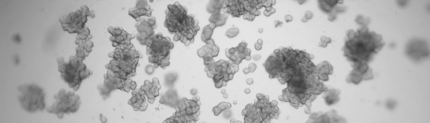
In Materials Science, transmission electron microscopy carrier grids can be used to prepare and observe the microstructure and morphology of various materials. Transmission electron microscopy (TEM) grids can provide sufficient support and fixation to prepare uniformly sized and shaped samples for observation and analysis in TEM. In addition, different types and sizes of TEM carriers can be used for specific experimental needs, such as electron beam etching and chemical etching.
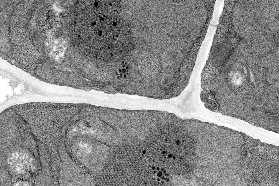
In Biology, the transmission electron microscope carrier network also plays a very important role. Biological samples often need to be sectioned or cut into very thin samples for observation in the transmission electron microscope. These sections must be placed on a carrier mesh and require special handling to ensure their structural integrity and observability. The use of a transmission electron microscope carrier mesh can improve the precision and reproducibility of sample preparation, as well as reduce errors and uncertainties during sample preparation and observation.
In Nanotechnology, transmission electron microscopy carrier grids are also widely used for the preparation and observation of nanomaterials. Nanomaterials usually have very small sizes and special structures, and the observation of these materials in a transmission electron microscope requires the use of a transmission electron microscope carrier mesh. The transmission electron microscope carrier mesh can provide sufficient support and fixation to prevent the deformation and movement of nanomaterials during preparation and observation. In addition, the use of different types and sizes of transmission electron microscope carriers allows for the positioning and quantitative analysis of nanomaterials.
As an important part of transmission electron microscope preparation and observation of samples, transmission electron microscope carrier network is of great significance for transmission electron microscope research and application. Its evolving techniques and methods have led to the increasingly widespread and in-depth applications of transmission electron microscopy in materials science, biology, nanotechnology, and other fields. In the future, with the continuous development and innovation of science and technology, the transmission electron microscope carrier network will also continue to improve the precision and efficiency of its preparation and use, and expand its application areas in materials science, biology and nanotechnology. At the same time, the structure and performance of transmission electron microscope carriers will be continuously optimized and improved to meet the preparation and observation needs of different samples, providing researchers with better experimental platforms and scientific tools.
We hope that this paper will help readers to understand the basic knowledge and important role of transmission electron microscope carrier network, and we also hope that researchers will pay more attention to the preparation and use of transmission electron microscope carrier network in their experiments, so as to make greater contributions to the progress of scientific research.
We offer Silicon nitride thin film windows / MEMS customization services. Feel free to leave a message to inquire.
Related Products

Related Reading
What is thin film deposition process
What is thin film deposition ? Thin film deposition technology is an important
Polycrystalline Silicon Thin Films丨Effects of Stress on Thin Films
Polycrystalline Silicon Thin Films丨Effects of Stress on Thin Films When thin films are attached to a substrate
Introduction of 3 applications of silicon nitride thin film windows in materials science
3 Application Scenarios of Silicon Nitride Thin Film Windows in Materials Science Silicon Nitride Thin
.jpg)