Chemical Vapor Deposition (CVD) Classification, Characteristics, and Applications
Chemical Vapor Deposition (CVD) is a technique in which a mixture of gases interacts with each other or with the surface of the substrate at a certain temperature and forms a thin film coating of metals or compounds on the surface of the substrate, so that the surface of the material can be modified to meet the requirements of wear, oxidation and corrosion resistance, as well as specific electrical, optical, tribological and other special properties. A technology.
Principles of CVD technology
CVD technology is based on chemical reaction, usually the reactants are gaseous and one of the products is solid is called CVD reaction, so its chemical reaction system must meet the following three conditions.
- At the deposition temperature, the reactants must have a sufficiently high vapor pressure. If the reactants are all gaseous at room temperature, the deposition device is relatively simple; if the reactants evaporate very little at room temperature, they need to be heated to evaporate them, and in some cases they need to be brought into the reaction chamber by a carrier gas.
- The reaction products must be gaseous, except for the required sediment, which is solid.
- The vapor pressure of the deposited film should be low enough to ensure that during the deposition reaction, the deposited film can be firmly attached to the substrate with a certain deposition temperature. The vapor pressure of the substrate material at the deposition temperature must also be low enough.
Classification of CVD technology
Classification by temperature
- Low-Temperature CVD (LTCVD): The deposition temperature is usually below 400°C and is suitable for temperature sensitive substrates.
- Medium-Temperature CVD (MTCVD): Deposition temperature between 400°C and 700°C.
- High-Temperature CVD (HTCVD): The deposition temperature is usually higher than 700°C, which is suitable for materials with high stability requirements at high temperatures.
Classification by pressure
- Atmospheric Pressure CVD (APCVD): CVD process at atmospheric pressure, simple equipment, but easy to lead to particle contamination.
- Low Pressure CVD (LPCVD): Performed in a low-pressure environment, it reduces particle contamination and improves film uniformity.
- Ultra-High Vacuum CVD (UHVCVD): Performed under ultra-high vacuum conditions, UHVCVD is suitable for the preparation of high-purity and high-quality films.
Classification by energy input method
- Thermal CVD (Thermal CVD): The formation of thin films by the decomposition or reaction of reactant gases through high-temperature heating.
- Plasma Enhanced CVD (PECVD): Utilizes plasma to reduce reaction temperature and improve deposition rate and film quality.
- Photo-assisted CVD (PACVD): The use of light energy (usually ultraviolet light) to promote chemical reactions, commonly used in the deposition of organic materials.
- Laser CVD (LCVD): The use of a laser beam to initiate or promote a chemical reaction, enabling localized fine deposition.
Classification by process characteristics
- Metal-Organic CVD (MOCVD): Uses metal-organic compounds as reactant gases and is widely used in the manufacture of semiconductors and optoelectronic devices.
- Vapor Phase CVD (VPCVD): uses gaseous compounds as reactants.
- Liquid Phase CVD (LPCVD): Uses liquid compounds as reactants, which usually need to be gasified first.
Applications of CVD
CVD technology plays a key role in several fields due to its flexibility and efficiency in the preparation of different materials and films.
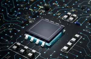
- Thin Film Deposition: CVD is used to deposit a variety of thin films such asAmorphous Silicon, polycrystalline silicon,Silicon Nitride (Si3N4), ,Silicon dioxide (SiO2)etc.
- LEDs and lasers: CVD is used to manufacture III-V semiconductor materials such as gallium nitride (GaN) and gallium arsenide (GaAs) in LEDs and lasers.
- Photovoltaic cells: CVD is used to deposit thin films in the manufacture of solar cells such assilicon filmand zinc oxide (ZnO), etc., to improve the photovoltaic conversion efficiency.
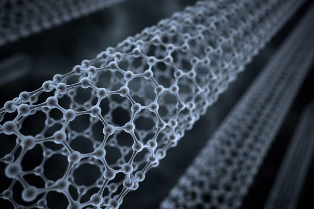
- Wear-resistant coatings: CVD is used to deposit superhard coatings such as diamond and cubic boron nitride (c-BN) to improve the wear resistance and service life of tools, molds and mechanical parts.
- Anti-corrosion coatings: CVD allows the deposition of corrosion-resistant coatings such asTitanium Nitride (TiN)and titanium carbide (TiC) for protecting metal surfaces from corrosion.
- Anti-Reflective Coating: CVD is used to prepare anti-reflective coatings to reduce reflections on the surface of optical elements and improve optical performance.
- Filters and Waveguides: In optical communications, CVD is used to manufacture devices such as filters and optical waveguides to improve signal transmission efficiency.
- Biocompatible Coatings: CVD technology is used to deposit biocompatible coatings such as titanium nitride and zirconium oxide (ZrO2) on medical device and implant surfaces to improve biocompatibility and durability.
- Micro-Electro-Mechanical Systems (MEMS): CVD is used to fabricate structural materials and functional films in MEMS devices, such as polysilicon and silicon nitride.
We have requests for customized films such as amorphous silicon, polycrystalline silicon, silicon nitride (Si3N4), silicon dioxide (SiO2), etc., or for foundry work for CVD processes such as ICPCVD (inductively coupled plasma) and PECVD (plasma enhancement).
Please contact us for any special requirements!
We offer Chemical Vapor Deposition (CVD) OEM Customization Services, Feel free to leave a message to inquire.
Related Products
Related Reading
Introduction of 3 applications of silicon nitride thin film windows in materials science
3 Application Scenarios of Silicon Nitride Thin Film Windows in Materials Science Silicon Nitride Thin
Variation of refractive index and absorption coefficient of amorphous silicon at different wavelengths
Variation of refractive index and absorption coefficient of amorphous silicon at different wavelengths In the study of the
Difference between LPCVD and PECVD
Difference between LPCVD and PECVD By high in low voltage environment
.jpg)