Principles and Advantages of Plasma Enhanced Chemical Vapor Deposition (PE-CVD)
PECVD technology is asCVDandPVDThe deposition temperature of PECVD technology is generally less than 600℃, which broadens the scope of application of substrate materials, and has the advantages of simple equipment, small deformation of workpiece, good performance of bypass plating, and uniform coating, etc. It not only overcomes the disadvantages of high deposition temperature of CVD technology, but also avoids the problems of poor bypass plating and complex equipment of PVD technology. PECVD technology overcomes the disadvantages of high deposition temperature and high requirements for substrate materials of CVD technology, and avoids the problems of poor winding plating and complex equipment of PVD technology, which is a new film preparation technology with great development prospects and application value.
Principle of PE-CVD
There are many kinds of plasma-enhanced chemical vapor deposition technology (PECVD for short), such as DC PECVD, pulsed DC PECVD, metal-organic compound PECVD, RF PECVD, microwave PECVD, arc light PECVD, etc. In recent years, with the cross-fertilization of various coating technologies, PVD and PECVD integrated composite deposition, particle nitriding and PECVD integrated composite deposition in the same furnace have been continuously developed. Of course, in recent years, with the cross-fertilization of various coating technologies, PVD and PECVD integrated composite deposition, particle nitriding and PECVD integrated composite deposition in the same furnace devices and technologies are constantly being developed. At present, most of the industrialized deposition of hard coating materials apply DC and pulsed DC PECVD technology.
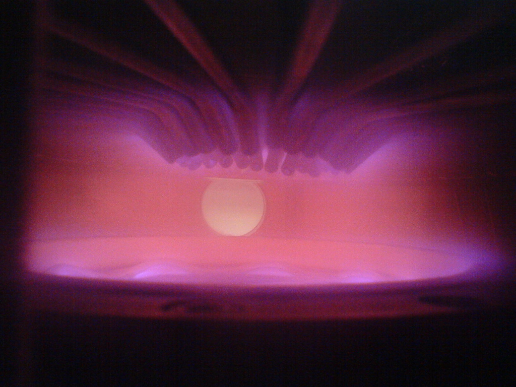
The earliest application of PECVD is accompanied by the development of the semiconductor industry and appeared for the processing of semiconductor materials, i.e., the use of silicone in the semiconductor material substrate deposition of Si02. later based on the characteristics of the PECVD process is particularly suitable for industrial production, the process began to be used in a large number of microelectronics industry (such as integrated circuit process, etc.), is mainly used in the deposition of large-area parts of the protective film and various insulating layers and DLC films. PECVD technology is the use of high-voltage electric field applied in the deposition chamber, so that the reaction gas in a certain pressure and excitation source (eg: DC high voltage, pulsed power supply, radio frequency or laser, etc.), electrons in the accelerating effect of the electric field to obtain energy, and the neutral particles in the gas (atoms or molecules occurring inelastic collision, and then the ionization of secondary electrons, which in turn further and the atoms in the gas, the secondary electrons, and the atoms in the gas. They are further and gas atoms and molecules in the collision ionization and produce electrons, so repeatedly collision and ionization, it will produce a large number of electrons and ions. Because of which the number of positive and negative particles are equal, it is called plasma. Charged particles in the collision process will also be due to the composite and transformed into neutral particles, and in the form of glow discharge to release excess energy. Reaction gas is excited into a very active molecular yard, ions and atomic groups composed of plasma, greatly reducing the deposition reaction temperature, accelerate the chemical reaction process to improve the deposition rate.
The reaction gas is excited into very active molecules, atoms, ions and atomic groups composed of plasma, which greatly reduces the deposition reaction temperature, accelerates the chemical reaction process and improves the deposition rate. Therefore, the general PECVD technology deposition temperature <600 ℃, broadening the scope of application of the substrate material, with simple equipment, small deformation of the workpiece, good performance around the plating, coating uniformity, modulation of the composition of the advantages of convenience. It overcomes the disadvantages of high deposition temperature of CVD technology and strict requirements on the substrate material, and avoids the problems of poor winding plating and complex equipment of PVD technology, which is very suitable for industrialized production. At present, PECVD is mainly used in MEMS industry (such as integrated circuit process) and the preparation of fine films. At the same time, PECVD technology is also used in binary optics, solar films, gradient refractive index optical films and anti-laser damage films with its good uniformity and step coverage, dense deposited films, high bonding of the film layer with the substrate, and fast deposition speed.
Advantages of PE-CVD
The PECVD method can be used to prepare different films by varying the process parameters, e.g., reactive gas flow rate, reactive gas ratio, RF power, chamber pressure, deposition temperature, film thickness, etc., which can lead to a great change in the film properties, especially in the optical and mechanical properties.
For example, for PECVD preparation of SiO2 films, when the RF power is increased, the activation rate of the reaction gas is increased, so the structure of the film will be relatively dense, and the uniformity will be improved accordingly. But when the power is too high, for the reaction will make the SiO2 generated by the deposition rate is too fast, but lead to the film structure is loose, vacuum density increases, repeatability will also decline, which will lead to poor uniformity, when the radio frequency power is too high, and even radiation damage to the substrate. Substrate temperature is also an important factor affecting the uniformity of the film, when the substrate temperature rises is, it will increase the energy of the particles deposited on the surface of the substrate, resulting in an increase in the mobility of the particles on the surface of the base, exacerbating the possibility of these particles traveling clusters or islands, which directly affects the uniformity of the film. On the other hand the elevated base temperature facilitates the filling of defects in the film surface by the particles.
Therefore, the PECVD method of preparing optical thin films has many advantages that other methods do not have.
(1) The reactants and by-products are gases, and the structure is simple compared to PVD and CVD equipment.
(2) Fast reaction deposition rate, especially for high refractive index thin film materials, such as a-Si, TiO2, etc.
(3) The composition of the film can be arbitrarily regulated to a large extent, and optical films can be obtained to prepare a variety of intermediate refractive index materials, such as SiCO:H, SiN:H, SiOxNy, SiOxFy, and so on.
(4) Structural integrity and denseness of the deposited film, good adhesion to the substrate
(5) Excellent Step Coverage
(6) Smooth deposition surface can be obtained
We offer Plasma Enhanced Chemical Vapor Deposition (PE-CVD) OEM Customization Services, Feel free to leave a message to inquire.
Related Products
Related Reading
Properties of diamond films and their applications
Properties of diamond films and their applications Diamond has a range of excellent properties
Silicon Nitride (SiNx) Thin Films for Optical Applications
Silicon Nitride Thin Film in Optics Silicon nitride thin film as a canonical
Influence of the annealing process on the platinum resistance
Influence of the annealing process on platinum resistors In the field of high-precision temperature measurement, thin-film
.jpg)