What are the characteristics and applications of vanadium dioxide prepared by magnetron sputtering

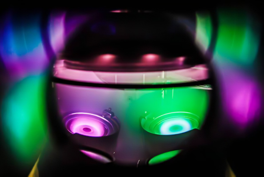
magnetron sputteringWidely used in the preparation of VO2 thin films, the target material is generally very pure vanadium metal, the background vacuum is generally higher than 10-3Pa, and the vacuum chamber is filled with oxygen and argon. Sputtering, Ar + ions bombardment V target sputtering V atoms and O atoms on the substrate surface combined and deposited to form vanadium oxides, the preparation of the film generally contain V2O3, VO2, V2O5 vanadium oxides, but by adjusting the oxygen partial pressure, deposition temperature and target base spacing, high-quality VO2 films can be prepared.
Characteristics of vanadium dioxide
Highly uniform and continuous film
Magnetron sputtering technology is capable of depositing material uniformly on a substrate, producing a continuous film without cracks or significant defects. This is particularly important to ensure the functionality of the film, as the consistency of the physical properties is critical to the thermal and electrical response of the VO₂.
Controlled film thickness and composition
By precisely controlling sputtering parameters such as power, air pressure, sputtering time and target-to-substrate distance, the thickness and composition of the film can be precisely adjusted. This is essential to achieve VO₂-specific phase change properties (e.g., transformation from insulator to metal at a specific temperature).
Excellent phase change properties
The main attraction of VO₂ films is their unique temperature-sensitive phase change capability, which can be effectively maintained and reproduced by magnetron sputtering. At ambient temperatures close to 68°C, VO₂ films can rapidly change from an insulating to a metallic state, a change that is accompanied by significant changes in conductivity and optical properties.
Improved optical and electrical properties
By adjusting sputtering conditions, such as substrate temperature and sputtering atmosphere (e.g., oxygen content), the structure of the film can be optimized to improve its optical transmittance and electrical conductivity. In smart window applications, for example, such optimization can improve their ability to regulate heat and light.
Higher material utilization and productivity
The high material utilization of the target material in the magnetron sputtering process and the fact that the equipment usually has a high deposition rate leads to higher productivity and lower production costs.
Wide range of substrate adaptations
Magnetron sputtering can be performed on many types of substrates, including glass, plastics, metals, etc., which extends the range of applications for VO₂ thin films, such as the possibility of applying them to bendable surfaces or objects with different shapes.
Environmentally friendly and low pollution
Magnetron sputtering is often considered a more environmentally friendly preparation method than other methods such as chemical vapor deposition, as it uses fewer precursors and does not involve the use of highly toxic chemicals.
Applications of Vanadium Dioxide
Vanadium dioxide terahertz device
The wavelength range of 0.03~3mm is defined as terahertz, which contains electromagnetic waves with frequencies in the range of 0.1THz to 10THz, between the microwave and infrared wavelength bands. In the very early days, Terahertz was known by different names in different fields. Far infrared was used in the optical field, while sub-millimeter waves, ultra-microwaves, etc. were used in the electronic field. Terahertz technology has been recognized as one of the "ten technologies that will change the world in the future". The phase transition of vanadium dioxide enables the absorption of specific frequencies of terahertz waves, utilizing this property of the material for switching purposes. On the one hand, due to the impedance of the film and the substrate and the external environment impedance is equal, the absorption structure will not produce reflection, so the terahertz wave will not be reflected; and terahertz wave resonance and the top layer of the metal ring structure to produce one or more peaks of absorption, and at the same time, the metal film so that the terahertz can not be passed through the device, and finally the absorptive rate of the absorber will be produced by the absorption rate of the changes to utilize the principle of such a fabrication of the absorber.
CD-ROM media material
Materials with bistable optical properties can be made into optical data storage media, and Vo2 film belongs to just such a material, and the transition between its two steady states is reversible, so it can be used as a readable, writable and erasable optical disk media material. It was found that the data stored in Vo2 films can be maintained for a long period of time and can withstand changes in ambient temperature and ultraviolet irradiation.
Optical Switching Devices
By utilizing VO2's resistance phase change amplitude of up to 5 orders of magnitude before and after the phase change and its nanosecond conversion time, it can be used as a thermal switch or a thermal sensor to realize automatic control of circuits. Optical switch using VO2 in the visible and infrared region of the transmittance of the sudden change, by adding some kind of excitation, and ultimately realize the transmission and reflection of the on and off, which is known as the light modulator. Terahertz wave is located in the microwave and infrared between electromagnetic waves, is the last electromagnetic spectrum to be developed in the spectral region, in the direction of broadband communications, biological sensing, semiconductor material properties of the research has great application value.
Laser protection layer for infrared detectors
Based on the great difference in IR transmittance before and after the phase transition of VO2, we can use VO2 film as a protective layer against IR laser radiation. When subjected to laser pulse radiation, it can rapidly undergo a metallic phase-semiconductor phase transition, with high infrared transmittance before the phase transition and very high infrared reflectance after the phase transition. In the absence of laser radiation, VO2 film shows high infrared transmittance, the normal operation of the infrared device does not have an impact; when subjected to laser radiation, VO2 film in the ultra-short period of time, the phase change to the metal state, at this time has a high infrared reflectivity, blocking the transmission of the radiation light, to achieve the purpose of the protection of the detector.
Smart Window Film Coating
When vanadium dioxide undergoes an insulator-metal phase transition, its optical properties also undergo a sudden change. This optical device coated with a thin film of VO2 is controlled when the externally supplied conditions of electricity, light, and heat induce a phase transition of the VO2 material, the high transmittance of the insulating state before the phase transition and the high reflectance of the metallic state after the phase transition, which is the principle of the vanadium dioxide material applied to the smart window. This vanadium dioxide smart window can realize reversible regulation with the effect of temperature on the phase transition. In particular, light from the infrared band can effectively prevent the absorption of external infrared light, thus maintaining a constant indoor temperature. On the contrary, when the outside temperature is lower than the temperature of the film's phase change, the transmittance of light increases, appropriately increasing the temperature of the room. Making full use of nature's gifts, the use of VO2 materials to flexibly regulate and maintain room temperature is beneficial to the goal of sustainable development.
We offer Magnetron sputtering foundry customization services, Feel free to leave a message to inquire.
What are the characteristics and applications of vanadium dioxide prepared by magnetron sputtering
What are the characteristics and applications of vanadium dioxide prepared by magnetron sputtering Magnetron sputtering method
Exploring 4 applications of silicon nitride thin-film windows in bioscience
This paper will describe the properties and advantages of silicon nitride thin film windows and discuss four common applications in the life sciences.
Science Guide: Introduction, Principle and Application Scenarios of Silicon Nitride Thin Film Windows
Science Guide: Introduction, Characteristics and Application Scenarios of Silicon Nitride Thin Film Windows Nitride


.jpg)