
Variation of refractive index and absorption coefficient of amorphous silicon at different wavelengths

Refractive index (n) and absorption coefficient (k) are two crucial parameters when studying the optical properties of amorphous silicon. These parameters not only reflect the material's response to light, but also directly affect the effectiveness of amorphous silicon in applications such as photovoltaic cells and sensors. By analyzing the refractive index and absorption coefficient at different wavelengths, we can gain a deeper understanding of the photovoltaic properties of amorphous silicon and how these materials can be optimized for specific technological needs.
Variation of refractive index (n) and absorption coefficient (k) of amorphous silicon at different wavelengths
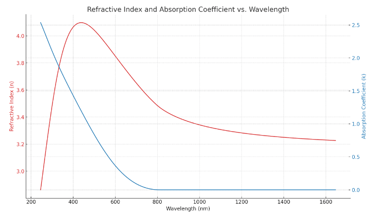
Refractive index map of existing amorphous silicon coating process
Features:
- Refractive index (n): reaches a high of 4.0 at 200 nm, decreasing to about 3.0 with increasing wavelength.
- Absorption coefficient (k): rises rapidly to 2.5 near 200 nm and then decreases rapidly with increasing wavelength.
This diagram shows the excellent absorption properties and high refractive index of amorphous silicon in the UV region. This property gives it potential for a wide range of applications in optics and photovoltaics, and is particularly suitable for technologies that require the utilization of UV light, such as in photocatalysis and medical devices.
Amorphous Silicon Thin Film Applications
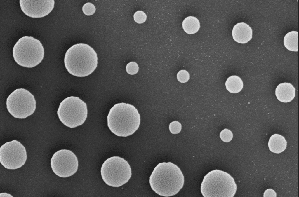
SEM image of an amorphous silicon superstructure lens
Optical Applications
- photovoltaic cell
- Liquid Crystal Display (LCD)
- optical sensor
- Waveguides and optical filters
- Anti-Reflective Coating
- heat detector
- Superlens
Among them, superlens is an optical element that can break through the optical diffraction limit and realize higher resolution than traditional lenses. Amorphous silicon thin films have important applications in the design and fabrication of superlenses due to their unique optical properties.
In the simulation design of the superlens, the amorphous silicon thin film process with high refractive index is selected as much as possible. Higher refractive index can not only effectively regulate the phase of light, reduce the thickness of the material, enhance the mechanical strength and thermal stability, thus reducing the manufacturing difficulty and cost, but also reduce the optical loss.
Please contact us for special customization requirements!
We offer Coating (micro- and nanofabrication) process customization services, Feel free to leave a message to inquire.
Physical Vapor Deposition (PVD) Classification, Characteristics, and Applications
Classification, Characteristics, and Applications of Physical Vapor Deposition (PVD) Physical Vapor
Difference between LPCVD and PECVD
Difference between LPCVD and PECVD By high in low voltage environment
Influence of the annealing process on the platinum resistance
Influence of the annealing process on platinum resistors In the field of high-precision temperature measurement, thin-film

.jpg)