What are the factors that influence the sputter coating process on thin film materials?

With high-energy particles (usually positive ions accelerated by an electric field) bombardment of the solid surface, the solid surface of the atoms, molecules and the incident high-energy particles to exchange kinetic energy from the solid surface splash out of the phenomenon known as sputtering. The sputtered atoms (or atomic groups) have a certain energy, they can be re-deposited cohesion on the surface of the solid substrate to form a thin film, known as sputtering coating.
Sputtering with thin film materials
The macroscopic properties of materials are closely related to their microstructure, so it is particularly important to use economical and effective methods to change the material's organizational structure so as to endow the surface of the material with new composite properties. In the early stage of thin film material preparation by sputter deposition, the influencing factors include the quality of the sputter source, the energy and angular distribution of the sputtered atoms, as well as the sputtering yield and rate. In the later stages of the preparation process, factors such as sputtering gas, sputtering voltage and substrate voltage, substrate temperature, target quality, vacuum and sputtering working air pressure are the main factors affecting the composition and organization of the thin film. While ensuring the stability of the thin film material organization, uniformity and purity are also important indicators that must be taken into account, as they are crucial for the selection and improvement of different sputter coating technologies.
Sputtering and material effects
1. Sputtering of metals and semiconductors
Secondary sputtering, tertiary sputtering, andmagnetron sputteringThese common sputtering methods are distinguished mainly by the electrode structure.
Ordinary DC two-stage sputtering is to apply a negative DC potential directly to the sputtering target and place the substrate frame of the coated workpiece as the anode. Atoms of the target material are sputtered from the cathode target and deposited on the surface of the substrate to form a thin film. In the sputtering process, the Ar discharge is in an abnormal glow discharge state, and the discharge glow covers the entire cathode target surface, making the target sputtering and substrate surface film formation uniform. In the abnormal glow discharge state, the deposition rate can be changed by adjusting the sputtering voltage and changing the sputtering current. The advantage of DC secondary sputtering is that the device is simple and suitable for sputtering metal and semiconductor targets. However, the deposition rate is low when sputtering; due to the high direct discharge voltage, the substrate is very easy to damage the temperature rise; the selection of air pressure conditions are harsh, low air pressure discharge can not be maintained, the quality of the film deposited by high air pressure is poor; sputtering insulating materials is not applicable.
DC tertiary sputtering is the introduction of a hot filament cathode and anode into a secondary sputtering device, with the filament cathode grounded and the anode 50-100 V. The filament emits electrons at high temperatures, which are accelerated by an electric field, and then collide and ionize with the Ar atoms in the process of moving toward the anode to create a non-self-sustaining hot cathode arc discharge. Three-stage sputtering can increase the discharge current, can completely control the ion current and ion charge independently, and can maintain the discharge at low voltage, which is superior to two-stage sputtering. At the same time, three-stage sputtering causes less radiation damage to the substrate and can be used to make thin films for integrated circuits and semiconductor devices. However, the structure of the device is more complex than that of cold cathode discharge, and it is difficult to prepare a plasma with a large coverage area and uniform density, and there are problems such as filament consumption, so this preparation process has almost ceased to be used in recent years.
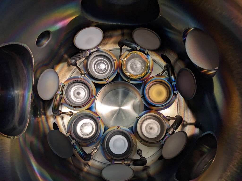
Magnetron sputtering technology is in the secondary sputtering cathode target surface to establish a ring-shaped closed magnetic field, it has a parallel to the target surface of the transverse magnetic field distribution, the magnetic field is generated by the target body of the magnet, is currently one of the mainstream technology for coating. Magnetron sputtering coating device structure is applied in the cathode target magnetic field, the use of the physical effects of the magnetic field on the bound electrons and effectively extend the electron trajectory, which increases the electrode and gas atom collision chances of enhancing the gas ionization rate, so that more energetic ions bombardment of the target material. According to the principle of magnetron sputtering can be seen, the key to magnetron sputtering technology is to establish an effective electron beam trap. Magnetron sputtering is a high-speed and low-temperature sputtering technology; its working gas pressure is 0.1 Pa, target current density can reach tens of milliamps, and the deposition rate reaches several hundred nanometers to 2000 nm per minute.
At present, magnetron sputtering coating technology has a wide range of applications in actual production, thanks to its significant features, namely, a wide range of dynamic adjustment of operating parameters, film deposition rate and thickness can be easily controlled; no droplet particle problem in the film layer; a wide range of target material selection, almost all metals, alloys and ceramic materials are available; the use of magnetron electrodes can effectively improve the sputtering rate. Therefore, the sputtering etching rate on the target surface and the film deposition rate on the substrate surface are both very high. At the same time, magnetron sputtering has the advantages of low energy sputtering substrate temperature is low. However, the traditional magnetron sputtering target using an uneven magnetic field, the local convergence effect of the plasma will lead to uneven etching. Moreover, the target material cannot have high magnetic permeability, which are the disadvantages of conventional magnetron sputtering.
2. Sputtering of insulating materials
From the device structure, DC sputtering and DC magnetron sputtering coating need to apply negative potential on the sputtering target, which requires the target material to be a good conductor, which is not applicable to the preparation of insulating dielectric film. In this regard, RF sputtering technology can be used to replace the DC sputtering device power supply with a RF power supply. In the sputtering process, the polarity of the power supply is switched according to the cycle, and the positive ions and electrons in the RF plasma between the target pole and the substrate bombard the insulating target alternately to produce sputtering.
RF sputtering avoids large scattering of atoms and improves the sputter deposition rate. At the same time, the sputtered particles have less energy loss during flight and higher energy when they reach the substrate, which is conducive to improving the bonding strength and densification of the film layer. At the same time, RF sputtering effectively reduces the dependence of discharge on secondary electrons and lowers the breakdown voltage, allowing sputtering of any material including dielectric materials. However, since the device structure of RF sputtering is not fundamentally different from that of secondary sputtering, there are also drawbacks such as low deposition rate, high substrate temperature and poor sputtering uniformity.
3. Compound thin film sputtering
The sputtering of alloys and compounds differs greatly from the sputtering of single-atom solids. Since the elements that constitute solids have different sputtering yields from each other, the preparation of compound thin films can be performed by the reactive sputtering method in addition to the radio-frequency sputtering method. That is, in the sputtering coating process, the reaction gas introduced at a later stage reacts with the target material sputtered and deposits on the surface of the substrate, obtaining a thin film with a composition different from that of the target material. The advantages of reactive sputtering are that the target material and the reactive gas can easily obtain high purity, which is conducive to the preparation of high-purity compound films; the composition of the film can be artificially adjusted to regulate the characteristics of the film; in the entire reactive deposition process, the substrate has a low temperature rise, which can be used for large-area homogeneous thin film preparation to achieve industrialized production. However, in the actual operation of the process, the preparation of compound targets is more difficult, the DC reaction sputtering process is unstable, the process is difficult to control easily caused by target poisoning, target source and workpiece surface flaming arc and other phenomena, these problems are serious constraints on the reaction sputtering technology development and promotion.
The phenomena of target poisoning, arc discharge and anode disappearance in reactive sputtering can be solved by changing the frequency of the sputtering target power supply. Medium frequency pulsed power supply has gradually become a new mode of power supply for compound reaction sputtering, and the frequency of this power supply is between DC and RF. In the mid-frequency AC magnetron reaction sputtering process, the two twin targets periodically alternate each other as cathode and anode under the action of suspended alternating current, so that they are sputtered in a cyclic rotation. The insulating film prepared by the mid-frequency reactive sputtering equipment is basically free of large particles compared with DC sputtering, and the film layer is denser. Moreover, the high deposition rate, stable working condition, low production cost and high substrate temperature in the sputtering process are conducive to the improvement of film quality and bonding force.
We offer Magnetron sputtering foundry customization services, Feel free to leave a message to inquire.
In-depth investigation: the differences and respective advantages of transmission electron microscopy and scanning electron microscopy
This paper will delve into the working principles, imaging methods and application areas of these two electron microscopes.
Polycrystalline Silicon Thin Films丨Effects of Stress on Thin Films
Polycrystalline Silicon Thin Films丨Effects of Stress on Thin Films When thin films are attached to a substrate
Polysilicon film丨Various factors affecting the surface properties of polysilicon film
Polysilicon Film丨Various Factors Affecting Surface Properties Growing Polysilicon Film


.jpg)