What are the properties and applications of silicon dioxide films prepared by electron beam evaporation?

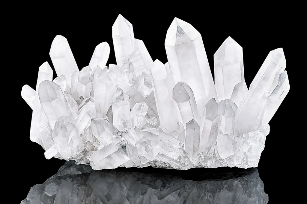
Silicon dioxide is an inorganic compound with the chemical formula SiO2, a compound of silicon and oxygen. It is widely found in nature and is one of the main components of many rocks and minerals, such as quartz, quartz sand, and glass. Silicon dioxide comes in a variety of forms, including crystalline and amorphous forms. Common crystalline forms include quartz, crystals and wollastonite, while the amorphous form is the main component of glass. Silicon dioxide has many important properties and characteristics that give it a wide range of applications in a variety of fields.
Process flow of silicon dioxide preparation by electron beam evaporation
1. System evacuation: First pump the deposition chamber to a high vacuum to reduce gas impurities and prevent oxidation.
2. Material loading: The silica block is placed in a crucible and placed within the focusing range of the electron gun.
3. beam of electronsGeneration and heating: A high-energy electron beam is emitted by an electron gun and focused onto the surface of the silica material, causing it to rapidly heat up to evaporation.
4. Thin film deposition: Evaporated silica molecules condense on the surface of the substrate material to form a uniform film.
Properties of Silicon Dioxide
physical property
1. Form: Silica exists in nature in a variety of crystalline forms, including quartz, crystal and flint. In addition, it can exist in amorphous forms such as glass or biogenic silica (e.g. diatomaceous earth).
2. Hardness: Quartz is one of the harder minerals in nature, with a Mohs hardness of about 7, making it ideal for use as an abrasive and wear-resistant material.
3. Melting point: Silica has a very high melting point of about 1710°C (quartz), making it useful in high-temperature applications.
4. Refractive index: Silica has a high refractive index (about 1.54), which makes it very important in the manufacture of optical components and glasses.
chemical property
1. Chemical stability: Silica exhibits very high chemical stability to most acids and bases at room temperature. However, it can be dissolved by hydrofluoric acid and reacts with strong bases to form silicates.
2. Insulation: Silicon dioxide is an excellent electrical insulator and is widely used as an insulating layer in electronic devices, especially in semiconductor manufacturing.
3. Thermal properties: Silica has good thermal stability and a low coefficient of thermal expansion, which makes it ideal for the manufacture of high-temperature-resistant materials and thermal protection layers.
Applications of Silicon Dioxide
Optical
In view of the excellent properties of silica film layers on silicon substrates, silica film layer structures on silicon substrates are usually utilized to design and fabricate active and passive optical waveguide devices. The use of silicon dioxide film preparation of optical waveguide devices can be a good match with the fiber optic mode field, fiber coupling loss is low, and easy to integrate, and to meet the general requirements of the integrated circuit design team optical waveguide, that is, single-mode transmission, transmission loss is low, and high efficiency of fiber coupling. Such devices have good conduction characteristics, and can achieve light amplification, light emitting and electro-optical modulation and other functions, is widely used in optical integration and optoelectronic integration.
Due to the low absorption and low refractive index of silica films, they are often used in conjunction with titanium oxide layers to form multilayered all-dielectric layers for the preparation of cold mirrors.TiO2/Si02 cold mirrors are able to withstand high temperatures, have a long service life, and have a number of advantages over ordinary infrared mirrors, such as the absence of diffuse green light, and the absence of a green halo in the resulting projected image.TiO2/SiO2 cold mirrors TiO2/SiO2 cooled mirrors have been widely used in projectors, copiers, and high power floodlights used in theaters.
TiO2/SiO2 multilayer film structure can also be used as an infrared reflective film, nowadays it is usually used as a lining layer for energy-saving lighting lamps in automobiles, which can effectively improve the luminous efficiency of the lamps, reduce the rate of light attenuation, prolong the service life, and provide a higher level of safety than the ordinary lamps.The infrared reflective properties of TiO2/SiO2 are also commonly used in architectural glass, which is capable of transmitting visible light and reflecting infrared light to minimize the thermal damage caused by infrared light, The infrared reflective properties of TiO2/Si02 are also commonly used in architectural glass, which can transmit visible light and reflect infrared light to minimize the thermal damage of infrared light.
In the field of anti-laser damage film research, Si02/TiO2 combined film system, the first layer of AR film with high refractive index film and the substrate between the first layer of the first layer of high refractive index film and the substrate firstly deposited a λ/2-thick layer of internal protection layer, will be 1.06 μm, 0.15 nm laser average damage value can be increased by 301 TP3T.
Microelectronics
Silicon dioxide thin film preparation process is highly feasible, its own insulation properties are good, and silicon dioxide has a variable forbidden band width, so that silicon dioxide has become the best material for non-products of silicon solar cell membrane layer, greatly improving the light absorption efficiency of solar cells, but also able to reduce the manufacturing cost of solar cells, to help the promotion of green energy.
In the process of preparing thin-film transistors (TFTs), it is necessary to prepare a thin film layer on a flexible polymer substrate without affecting the chemical properties and surface morphology of the polymer substrate. Silicon dioxide, with its unique properties and a variety of preparation methods, is the only choice for the manufacture of the gate dielectric layer in thin-film transistors.
In the preparation of silicon high-power bipolar body tube process, if the use of silicon dioxide film layer to make the body tube core in the plane and table surface passivation, can improve or maintain the breakdown voltage of the transistor core, and can protect the passivation device, in order to ensure that the transistor is stable at the same time to achieve the effect of preventing external contamination, in the disturbance, to ensure the reliability of the device.
Other areas
Amorphous silica films are also used as inorganic electret materials in electret electroacoustic devices, sensor devices, solar panels, motors and generators.
Amorphous silicon dioxide film of negative charge charging and storage capacity is good, charge storage life is long, able to resist high temperature and other harsh environments, and easy to combine with modern silicon semiconductor process to make the inorganic electret device miniaturization, and realize the integration of the circuit.
Silicon dioxide film layer can also be used as ITO transparent conductive glass species of sodium ion blocking layer, due to the preparation method is simple and easy to carry out mass production and process parameters are stable and controllable, has been able to carry out industrialized mass production.
In view of the excellent characteristics of silica material, can be sol-gel technology to dip coating silica film on the glass surface, because in the preparation process of silica in the gel state, can be formed in the microporous and cracks in the gelation effect, fill the holes in the surface of the material, can narrow and passivate the cracks on the material, so that the subsequent heat treatment of the glass, the technology can be used for the strength of the material in terms of modification.
In addition, amorphous silica film layers are superior packaging materials for high-resistance food packaging.
We offer Coating (micro- and nanofabrication) process customization services, Feel free to leave a message to inquire.
Silicon nitride thin film window applications Materials Science丨Semiconductor丨Bioscience
Silicon nitride thin film window products are used in a wide range of applications in materials science, semiconductor production and analysis, and bioscience. Our high quality products provide high resolution imaging capabilities for a wide range of sample types and sizes.
PECVD vs. magnetron sputtering: which technique is better for preparing amorphous silicon thin films?
PECVD vs. magnetron sputtering: which technique is better for preparing amorphous silicon thin films
How to choose the right silicon nitride thin film window丨Science Guide
With this guide, you can make informed decisions to optimize your TEM imaging, SEM analysis, bioscience research, or semiconductor production.


.jpg)