Magnetron sputtering丨process for making platinum temperature sensors
Magnetron sputtering丨process for making platinum temperature sensors In the field of modern technology, the

Silicon nitride thin film windows are widely used not only in bioscience but also in materials science as a thin film material with high transparency, high stability, high corrosion resistance and high hardness for characterization and analysis in the materials science field. In the following, we will learn about the properties of silicon nitride materials and introduce the applications of silicon nitride thin-film windows in materials characterization, materials analysis, and materials reaction studies, respectively.
Silicon nitride is a ceramic material with excellent mechanical, thermal and electrical properties properties and is transparent, making it ideal for the fabrication of thin film windows for various analytical techniques such as scanning electron microscopy (SEM) and transmission electron microscopy (TEM).
One of the main advantages of using silicon nitride thin-film windows is their ability to withstand high temperatures and pressures. This is particularly important for materials science applications that study materials under extreme conditions, such as in aerospace, energy and other high-tech industries. Silicon nitride windows can withstand temperatures of up to 1200°C and pressures of up to 200 atmospheres, allowing researchers to study materials under conditions that are not possible with other types of windows.
Another advantage of silicon nitride thin-film windows is their superior optical clarity. They are virtually transparent, enabling researchers to observe materials with a high degree of precision and detail. This is particularly useful for studying the microstructure of materials and analyzing the behavior of materials at the atomic and molecular levels.
Silicon nitride windows are also known for their high durability, making them the most cost-effective solution for many applications. They are resistant to acid and alkali corrosion and can withstand strong acid and alkali chemicals, making them ideal for a variety of industrial and scientific applications.
The main application of silicon nitride thin film windows in materials characterization is the sample support film for transmission electron microscopy (TEM) and scanning transmission electron microscopy (STEM). Transmission electron microscopy is a very important characterization tool to observe the microstructure and chemical composition of samples, which is important for research in the field of materials science.
As a sample support film for transmission electron microscopy, silicon nitride thin film windows can provide high transparency, high stability and high resolution imaging, which facilitates researchers to observe the microstructure and chemical composition of samples. In addition, silicon nitride thin film windows are also used in in situ transmission electron microscopy studies to investigate the microstructure and kinetic behavior of materials under high temperature, high pressure, and high resolution conditions.
The main application of silicon nitride thin film windows in materials analysis is as a sample support film with X-ray diffraction (XRD), atomic force microscopy (AFM) and other techniques to analyze the surface morphology, structure and properties of the material.
X-ray diffraction is a widely used technique in materials science to study information such as crystallinity, crystal structure and lattice parameters of materials through diffraction patterns. The silicon nitride thin film window is used as a sample support film, which allows the distance between the sample and the X-ray to be reduced, resulting in a better diffraction pattern. In addition, silicon nitride thin film windows can also be used for sample preparation and analysis in atomic force microscopy (AFM), where information such as roughness and frictional properties of the material surface can be obtained by AFM analysis techniques.
Researchers can use transmission electron microscopy (TEM) and scanning electron microscopy (SEM) techniques to observe chemical reactions on material surfaces and use silicon nitride thin-film windows to obtain high-resolution images and videos. In addition, the high corrosion resistance of silicon nitride thin-film windows makes them ideal for observing high-temperature reactions and reactions in strongly acidic or alkaline environments.
In addition, silicon nitride thin-film windows can be used to study the electrochemical reactions of materials. Electrochemical reactions are an important field in materials science and chemical engineering, involving the conversion of electrical energy into chemical reaction energy. The high electrical conductivity and transparency of silicon nitride thin-film windows make them ideal for studying electrochemical reactions, allowing real-time monitoring of the process and studying the mechanism of electrochemical reactions.

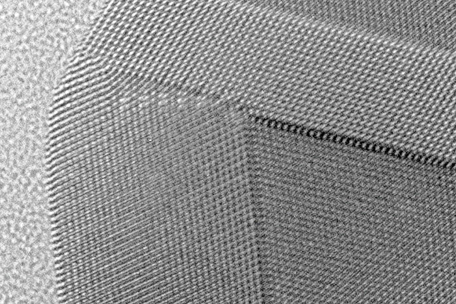
-Atomic-resolution-TEM-images of triple and quadruple lines at the interface between the Σ3-boundary and -Σ9-boundary.H.-Rosner- and -C.-Kubel- et al. Journal of Materials, 2011-59-7380-7387.jpg
Overall, silicon nitride thin-film windows have a wide range of applications in materials science and offer unique advantages such as high light transmission, high chemical stability, and high temperature tolerance. In material analysis, reaction studies, and growth monitoring, silicon nitride thin-film windows can provide very important information to help researchers gain insight into the properties and reaction mechanisms of materials.
At the same time, it also has a wide range of applications in biological sciences, electronics, optics and other fields. With the continuous development of technology, the application of silicon nitride thin-film windows in materials science will be continuously expanded and improved to make greater contributions to the development of materials science.
We offer Silicon Nitride Thin Film Windows / MEMS Customization Services, Feel free to leave a message to inquire.
Magnetron sputtering丨process for making platinum temperature sensors In the field of modern technology, the
Silicon nitride thin-film windows have become an important part of the semiconductor industry due to their unique properties. Silicon nitride thin film windows have a wide range of applications, from production to analysis, and play a key role in the development of new semiconductor devices and materials.
Difference between LPCVD and PECVD By high in low voltage environment
.jpg)