Properties of diamond films and their applications
Diamond has a series of excellent properties, including the highest known hardness, modulus of elasticity wear resistance, very high resistivity, breakdown field strength and low dielectric constant, wide spectral transmission range, very high thermal conductivity, very low coefficient of linear expansion, a very wide bandwidth, very high carrier mobility, and very good chemical stability, etc., so diamond has always been a material of great concern to the people with excellent performance and application prospects. diamond has been a material of great interest with excellent properties and application prospects.
Sources of Diamond Films
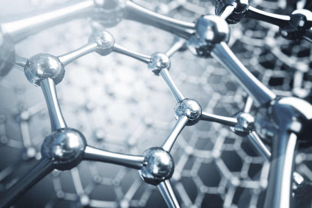
Carbon in the form of amorphous carbon black, graphite, carbon - 60 (C60), diamond four isotopes exist in which graphite is composed of six carbon atoms to sp2 bonds to form a honeycomb 6-atom ring, many of the 6-atom ring connected to layer, and then layer and layer connected to form a layered structure of the graphite crystals; Carbon - 60 (C60) is composed of sixty carbon atoms to form a spherical structure of the crystals; in the crystal structure of diamond In the crystal structure of diamond, each carbon atom is sp bond hybridization orbital with four carbon atoms to form covalent single bond. four carbon atoms arranged in the tetrahedron cone angle top, and each top corner of the tetrahedron are adjacent to the four tetrahedrons in common. Isomers have completely different properties due to their different structures.
Between 1952 and 1953, Eversole in the United States used the cyclic reaction method to decompose carbon-containing gases at 600~1000℃ and 10~100Pa gas pressure to grow diamond on diamond seed crystals, confirming for the first time that diamond can also be prepared under low gas pressure conditions. Using this cyclic high-temperature thermal decomposition method often requires diamond as a substrate, diamond belongs to the homogeneous epitaxial growth, coupled with the cyclic process, which reduces the deposition rate of diamond (~1nm/h), so it is very unsatisfactory. 1955 General Electric Company (GE) for the first time in the United States using high temperature and high pressure method (HTHP) to create artificial diamond. Due to its hardness and wear resistance, synthetic diamond has a wide range of applications in industry, including cutting or processing mechanical parts polishing or grinding optical materials. However, high temperature and high pressure method (HTHP) also has big disadvantages, mainly HTPT method on the equipment requirements of harsh, high cost, the manufacture of artificial diamond are the size of nanometers to millimeters between the small single-crystal particles, can not be used in conventional methods to be forged, processed, molded, and can not be made into a film-like diamond, and therefore can only take advantage of the characteristics of its high hardness, which restricts the excellent properties of diamond The development and utilization of diamond's excellent properties are limited.
In 1968 Angus et al. prepared diamond films on natural diamond using low-temperature, low-pressure chemical vapor deposition (CVD), and found for the first time that the presence of hydrogen atoms during the deposition process preferentially etched graphite over diamond.In 1982 Matsumoto et al. made a breakthrough in chemical vapor deposition (CVD) diamond film technology by using a hot wire (~ 2000°C) to activate hydrogen and carbon compounds in the vicinity of the hot filament to deposit diamond onto a non-diamond substrate 10 mm away from the hot filament. During the deposition of diamond, graphite is etched by hydrogen atoms, thus eliminating the process of alternating cycles of deposition and etching required by the cyclic reaction method, increasing the growth rate of diamond films, and also improving the quality of diamond films on non-diamond substrates. Since then, various CVD diamond thin film preparation techniques have emerged, improved and perfected. The role of atomic hydrogen in the growth of diamond films is also being gradually recognized. The growth rate of diamond is also gradually approaching the requirements of industrialized standards. In addition to chemical vapor deposition (CVD), physical vapor deposition (PVD) is also capable of depositing diamond films.
Mechanical and acoustic properties of diamond thin films and their applications
Diamond has excellent mechanical and acoustic properties. Diamond has a hardness of 100 GPa, the largest of any known material. The high hardness and wear resistance of diamond, combined with its extremely low coefficient of friction, make diamond an excellent tool material. By depositing diamond film directly onto the tool surface, diamond coated tools with different geometries can be prepared, showing the superiority of long life, fast cutting rate, high machining accuracy, high machining quality, etc. They have better performance than the traditional carbide tools, and they have a broad application prospect in the field of machining non-ferrous materials. Nowadays, there have been inlaid tools made of cut diamond thick film and diamond film coated tools sold in the market, successfully used for cutting non-ferrous, rare metals, graphite and composite materials especially suitable for aviation, automotive industry used in the cutting and processing of high silicon aluminum alloy materials.
Diamond has a large modulus of elasticity, Young's modulus, and is also the fastest material of all substances in terms of body acoustic wave and surface acoustic wave speed. At present, surface acoustic wave (SAW) devices have been successfully used in satellite communications, mobile communications, fiber optic communications and many other aspects. In recent years, with the demand for high-capacity data transmission, the demand for high-frequency SAW devices is increasing day by day, from the initial MHz level to the current GHz level. the frequency of the SAW device is directly proportional to the acoustic propagation velocity of the material, inversely proportional to the period of the fork finger transducer (IDT). In recent years it has been gradually recognized that the deposition of piezoelectric thin films on high acoustic velocity substrate materials constitutes a layered structure that can increase the SAW broadcast speed.
From 1989 to the present, Japan, Europe and the United States have begun work on high-frequency SAW devices with diamond film as the substrate, and some research progress has been made. Through different piezoelectric materials deposited on the diamond film substrate, SAW devices with structures such as ZnO/diamond/Si, Si02/ZnO/diamond/Si, AlN/diamond/Si, LiNbO3/diamond/Si, LiTaO3/diamond/Si, etc., were formed, and the comprehensive performance of the devices is being The overall performance of the devices is improving. It is predicted that if the preparation process is further improved, the frequency of diamond film SAW devices can reach 10GHz or even higher. Diamond film high frequency SAW filters are not only higher than traditional SAW filters in frequency, but also better than traditional SAW filters in power durability and high fidelity transmission.
In addition, the diamond film deposited on the vibration plate of the speaker member as the diaphragm of the high unit of the hi-fi speaker has a greater speed of sound and Young's modulus than ordinary vibration film, and it is the preferred material for high-grade audio speakers.
Thermal properties of diamond films and their applications
In recent years, modern electronic devices and circuits are developing in the direction of high integration, high speed, multi-functionality and high power consumption. Hundreds of millions of components on a chip, IC integration continues to improve, the size of individual components continue to shrink, on the one hand, there is a great potential for application and economic benefits, on the other hand, also led to a significant increase in the device and circuit heat dissipation per unit volume. For example, the heat generated by a single chip has increased from the original 10W to 40W; traditional emitter-coupled logic (ECL) circuits will be as high as 50W/cm2 heat flux; and dynamic randomized memory will be 20W/cm2 heat flux. Integrated circuit packaging shell is the chip's thermal conductivity channel, so the development of microelectronics technology requires the production of packaging shell of the substrate material has a very high thermal conductivity, in order to chip in a timely manner the heat generated by the heat emitted. Diamond has many excellent characteristics, the most prominent of which is its thermal conductivity in all materials is the highest, up to 20W/cm-K.
Diamond belongs to the phonon thermal conductivity, at room temperature diamond's thermal conductivity rate is more than 4 times higher than the current copper material used in most heat sinks. At the same time, the specific heat of diamond is very small, can not accumulate thermal energy, and can withstand sudden cold and sudden heat when the thermal shock, so it is an excellent heat sink material. In addition, the coefficient of thermal expansion of diamond is very close to that of silicon, which is very suitable for use with integrated circuits, and studies have shown that the permissible power usage capacity of diamond is 2,500 times higher than that of silicon. At the same time, diamond has a much lower dielectric constant than all currently developed high thermal conductivity substrates, such as BeO, AL2O3, AIN and SiC. In addition, diamond forbids bandwidth and has an extremely high resistivity (1014 Q-cm) at room temperature. These properties, combined with the highest hardness, good mechanical properties, chemical stability, frequency stability and excellent temperature stability that diamond possesses, make diamond the most ideal material for heat dissipation and heat sink encapsulation.
In recent years, the development of diamond film preparation technology has made the application of diamond film deposition on large-scale integrated circuits and high-power semiconductor devices a reality. Currently, CVD diamond films have been commercialized as heat sink materials for high-power semiconductor laser diodes.
Optical properties of diamond films and their applications
With a forbidden band width of 5.5eV, diamond has high spectral transmission properties from 225nm to the far infrared, coupled with diamond's high hardness, strength, thermal conductivity, and extremely low coefficient of linear expansion and good chemical stability, the combination of these excellent properties makes diamond films an excellent optical window material that can be used in harsh environments. Diamond films can be used as optical window materials in a wide range of wavelengths from the ultraviolet to the far infrared in two applications, i.e., as a window alone or as a window coating on other materials. Typical infrared optical window materials in the wavelength range of 8-12 μm are ZnS, ZnSe and Ge. Although these materials have excellent infrared transmittance, they are easily damaged due to their brittleness and other drawbacks.
With high transparency high chemical resistance and strong thermal shock resistance, diamond is a more desirable material for infrared windows. For example, many current window materials for infrared optics utilize high growth rate, high quality self-supported diamond films. The refractive index of diamond is 2.41, higher than typical dielectric materials, but lower than most semiconductor materials diamond than silicon, germanium, II-VI compounds, lead salts and other materials used in infrared detectors, the refractive index is lower, diamond film as a coating layer for infrared devices, it is a very potential application of the material. In addition, it is analyzed that the efficiency of silicon solar cells can reach 40%, while germanium solar cells coated with diamond film can reach 88%.
At present, diamond film is not only used for infrared optical window materials, permeability enhancement film, but also can be used to do visible optical window and X-ray lithography mask materials.
Electrical properties of diamond films and their applications
Due to the wide width of the diamond forbidden band, electron and hole mobility is very high, coupled with a high breakdown electric field, dielectric constant is small, resistivity, thermal conductivity and other characteristics, very suitable for highly integrated semiconductor devices at high temperatures, high bias, high power, high radiation conditions. Therefore, it is expected to replace silicon, used as an ideal material for the preparation of high temperature, radiation and other harsh conditions such as the preparation of electronic devices.
Since 1994 the RD42 research group, funded by the European Center for Particle Research (CERN), has carried outChemical vapor deposition method (CVD)Made diamond for charged particle tracking research work. After several years of research made some progress they used CVD diamond films to obtain microstrip array detectors and pixel array detectors, and studied the performance of these detectors in the detection of high flux mesons, neutrons, protons, y-rays, X-rays and ultraviolet light. The results show that the electrical properties of diamond do not degrade even under high-dose particle and again-ray irradiation. The study shows that diamond detectors are highly resistant to radiation and can work in extremely harsh environments (high temperature, strong chemical corrosion), and have good applications in high-energy physics experimental setups, space charged particle measurements, earthquake forecasting, radiation medicine, and nuclear technology applications.
In recent years, it has been found that diamond has the properties of negative electron affinity potential, switching function, and the ability to realize a certain degree of p-type doping and n-type doping, etc., and relevant application research has been carried out around these properties, and certain progress has been made, such as for flat panel displays with field emission cold cathode preparation has been a hot research topic in recent years in the international academic community, and the diamond thin film is a very promising cathode for flat panel displays. Diamond film is a promising cathode material for flat panel display, which can be used to manufacture cold cathode electron emitter and flat panel display, and the United States, Japan and other countries have invested a lot of human and financial resources.
Due to the difficulty of obtaining good n-type doping in diamond, realizing diamond bipolar p-n junctions is difficult to achieve for the time being. The current research focuses mainly on metal semiconductor field effect transistors (MESFETs) and metal insulator field effect transistors (MISFETs).
CVD diamond films can also be used to prepare fast optical switches (60 ps) under high bias conditions have aerospace and military applications.
We offer Chemical Vapor Deposition (CVD) OEM Customization Services, Feel free to leave a message to inquire.
Related Products
Related Reading
Science Guide: Introduction, Principle and Application Scenarios of Silicon Nitride Thin Film Windows
Science Guide: Introduction, Characteristics and Application Scenarios of Silicon Nitride Thin Film Windows Nitride
In-depth investigation: the differences and respective advantages of transmission electron microscopy and scanning electron microscopy
This paper will delve into the working principles, imaging methods and application areas of these two electron microscopes.
Physical Vapor Deposition (PVD) Classification, Characteristics, and Applications
Classification, Characteristics, and Applications of Physical Vapor Deposition (PVD) Physical Vapor
.jpg)