
In-depth investigation: the difference between transmission electron microscopy (TEM) and scanning electron microscopy (SEM)
Transmission electron microscopy (TEM) and scanning electron microscopy (SEM) are indispensable tools in modern scientific research. Equipped with higher resolution than optical microscopes, electron microscopes observe and study the microstructure of samples with high resolution and magnification by using signals generated by the interaction of electron beams with matter. Enabling researchers to obtain critical information that is difficult to obtain by other methods.
Transmission electron microscopy and scanning electron microscopy play an important role in many fields such as materials science, biology, and nanotechnology. In this paper, we will compare the working principles, imaging methods and application areas of transmission and scanning electron microscopes to help readers choose the equipment more suitable for their research fields.
What is transmission electron microscopy?
Transmission electron microscopy, or Transmission Electron Microscope (TEM) is a high-resolution microscope that uses the transmissive nature of the electron beam to observe the internal structure and details of a sample. Unlike optical microscopes, TEMs use an electron beam rather than a light beam because electrons have shorter wavelengths and can overcome the diffraction limitations of light beams, thus providing higher resolution.
How does transmission electron microscopy work?
Transmission electron microscopy (TEM) works on the principle of wave-particle duality of electrons. In a TEM, electrons are generated from an electron gun and focused through a series of lens systems. The sample is placed in a sample chamber in the TEM and the electron beam passes through the sample and into the projection chamber. In the projection chamber, the electron beam interacts with the sample, with some of the electrons being scattered by the sample and others passing through the sample. Transmission electron microscopy (TEM) typically has a higher resolution capability than scanning electron microscopy (SEM). This is because TEM uses transmitted electrons to form an image, and electrons have shorter wavelengths, which allows TEM to observe smaller details and produce images of the sample with high resolution.
The strength of transmission electron microscopy lies in its high resolution and ability to observe internal structures. It provides atomic-level resolution, enabling scientists to study details such as the crystal structure of materials, atomic arrangements and lattice defects. Transmission electron microscopy is used in a wide range of applications in materials science, nanotechnology, biology and chemistry
What is Scanning Electron Microscopy?
Scanning Electron Microscope (SEM) is a high-resolution microscope that observes and analyzes the surface topography and composition of a sample by using the interaction of an electron beam with the sample. Unlike conventional optical microscopes, SEM uses an electron beam instead of a light beam and uses scattering and detection signals to generate images.
How does the SEM work?
The SEM works based on the interaction of electrons with the sample. The electron beam is generated from an electron gun and passes through a series of focusing and scanning systems for beam diameter control and sample scanning. When the electron beam hits the sample surface, the electrons interacting with the sample produce a variety of signals, including secondary electrons, reflected electrons, scattered electrons, and X-rays.
These signals are captured by the detector and converted into a visual image by an image processing system.The SEM gradually forms an image of the entire sample by scanning the sample surface and acquiring signals at each location. The image has high resolution and surface topological detail and can be used to analyze features such as sample morphology, texture, particle distribution and tissue structure.
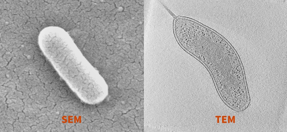
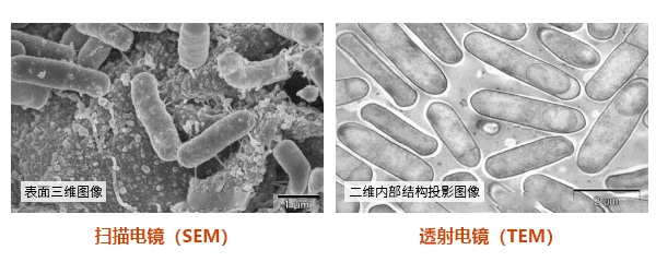
Transmission electron microscope and scanning electron microscope difference
| Scanning Electron Microscope (SEM) | Transmission Electron Microscopy (TEM) | |
| Electronic Type | Scattered scanned electrons | Transmission electrons |
| Image formation | Electrons are captured and counted by the detector Display on PC computer screen | Imaging directly on a fluorescent screen or on a PC computer screen using a charge-coupled device (CCD) |
| Image information | Surface 3D images | Two-dimensional internal structure projection image |
| Maximum multiplier | About 1-2 million times | More than 50 million times |
| Optimal spatial resolution | Approx. 0.5 nm | Less than 50 pm |
| Maximum field of view | Large | Limited |
| Sample thickness | Unrestricted | Usually <150 nm |
| High Pressure | 1-30 kV | 60-300 kV |
| Difficulty of operation | Easy to use, little or no sample preparation required | Not easy to use, requires sample preparation and training prior to use |
| Cost | Cheaper | more expensive |
| Speed | Quick | slow |
Which electron microscope is better for you?
When choosing the right electron microscopy technique for you, different factors need to be considered to determine the most appropriate choice. The following are some considerations that can help you make your decision:
Purpose of analysis
The first step is to determine what the purpose of your analysis is. Different electron microscopy techniques are suitable for different types of analysis. If you are concerned with sample surface characteristics, such as roughness or contamination detection, then scanning electron microscopy (SEM) may be more appropriate for you. And if you want to understand the crystal structure of your sample, detect structural defects or impurities, then transmission electron microscopy (TEM) may be more appropriate.
Image Type
SEM provides a detailed 3D image of the sample surface, while TEM provides a 2D projected image of the internal structure of the sample. You need to consider your information needs for the sample and your ability to interpret the images. If you are more comfortable interpreting 3-D images, then SEM may be better for you. However, it is important to note that the interpretation of the 2D projected image of the TEM may be somewhat difficult.
Sample Type
SEM and TEM have different adaptations for different types of samples. SEM is suitable for solid, liquid and biological samples, while TEM is mainly used for solid samples and can also be used to observe liquid samples by encapsulating the sample with a silicon nitride film window. For non-conductive samples, additional processing (e.g., metal coating) may be required to improve conductivity for observation in the SEM. In addition, biological samples require special curing and sectioning in the TEM.
Sample Preparation
Another important consideration is the complexity of sample preparation. SEM samples typically require little or no preparation, and SEM is more flexible in terms of sample size requirements and can be mounted directly on the sample stage for imaging. In contrast, the TEM sample preparation process is much more complex and requires experienced and trained users to operate. The sample must be very thin, below 150 nm or even below 30 nm and as flat as possible, without introducing any artifacts or unwanted variations during the preparation process. This means that TEM sample preparation may require more time and skill.
Resolution requirements
Depending on your analytical needs, you may have specific requirements for the resolution of your images. In this regard, the TEM typically has higher resolution capabilities than the SEM. If you need to perform high-resolution imaging, especially for the observation of fine structures, the TEM may be more suitable.
In summary, choosing the right electron microscopy technique depends on the purpose of your analysis, your preference for image type, the complexity of your sample preparation, and the resolution required. Understanding these factors and matching them to your specific needs will help you make an informed choice and obtain accurate, detailed microscopy images to support your research.
We offer Silicon nitride thin film windows / MEMS customization services. Feel free to leave a message to inquire.
Related Products

Related Reading
Process Principles and Applications of Optical Coatings
Principles and Applications of Optical Coating Technology The process principles of optical coating mainly involve
Magnetron sputtering丨understanding the principle, classification and advantages
What is magnetron sputtering? Magnetron sputtering is a commonly used method of PVD thin film production.
Difference between LPCVD and PECVD
Difference between LPCVD and PECVD By high in low voltage environment
.jpg)