Difference between ICPCVD and PECVD preparation of silicon nitride films

ICPCVD (Inductively Coupled Plasma Chemical Vapor Deposition) andPECVD (Plasma Enhanced Chemical Vapor Deposition)are two common techniques used to prepare silicon nitride (SiNx) thin films. Although both are plasma-enhanced chemical vapor deposition methods, they have some important differences in plasma generation, film characterization, and applications.
Principle and Equipment
ICPCVD
- Plasma Generation: Inductive coupling is used to generate a high density plasma in a coil, usually by RF (Radio Frequency) power. The plasma is formed in a vacuum chamber and directed to the surface of the substrate.
- Plasma Density: ICPCVD produces a higher plasma density, which provides higher ion bombardment energy.
- Equipment complexity: ICPCVD equipment is complex and expensive due to the need for sophisticated coil and power control systems.
PECVD
- Plasma generation: capacitive coupling is used to generate plasma between two electrodes, usually by RF power.
- Plasma Density: PECVD produces a relatively low plasma density, but it is still sufficient to facilitate chemical reactions and thin film deposition.
- Equipment complexity: PECVD equipment is relatively simple, low cost and easy to operate and maintain.
Thin Film Properties
- Film Density: Due to the high plasma density, ICPCVD is able to deposit silicon nitride films with high density and low porosity, while PECVD films have a relatively low density.
- Chemical purity: films deposited by ICPCVD typically have higher chemical purity and lower levels of impurities. films deposited by PECVD may contain more hydrogen and other impurities, but this can be improved by post-processing.
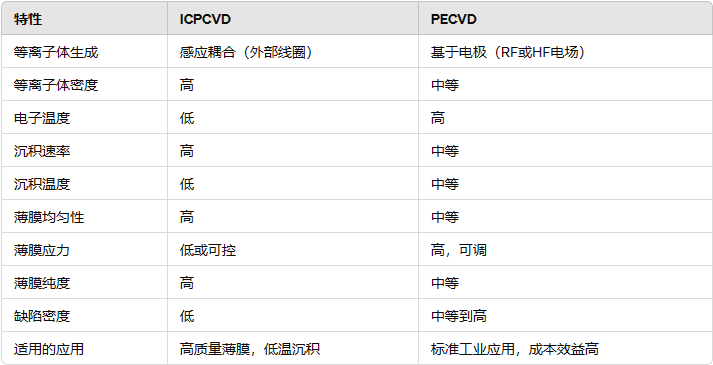
Comparison of characteristics

Applications
ICPCVD
- High-performance optical coatings: Due to the high film densities and low stress characteristics, ICPCVD is suitable for high-performance optical coatings such as anti-reflective and protective coatings.
- Semiconductor devices: ICPCVD is advantageous in semiconductor devices with high precision and reliability requirements, such as MOSFETs and MEMS devices.
- High-quality insulating layers: For insulating layers requiring high dielectric strength and low leakage current.
PECVD
- Large Area Coating: PECVD is suitable for large area and fast deposition applications such as solar cells and display backsheets.
- Multilayer thin film structures: PECVD is suitable for the preparation of multilayer thin film structures such as in flat panel displays and optoelectronic devices.
- Low temperature applications: For temperature sensitive substrates such as organic and plastic substrates.
ICPCVD and PECVD each have their own advantages and areas of application, and the choice of method depends on the specific application needs and process requirements. ICPCVD has advantages in terms of high density, low stress, and high purity films, while PECVD performs better in terms of large area, fast deposition, and cost control. By understanding the differences between these two methods, you can discuss with our researchers and engineers to choose the most appropriate deposition process for your needs.
We offer Coating (micro- and nanofabrication) process customization services, Feel free to leave a message to inquire.
Thin film nucleation and growth
Thin Film Nucleation and Growth Thin film nucleation and growth is a central step in coating technology.
Magnetron sputtering丨understanding the principle, classification and advantages
What is magnetron sputtering? Magnetron sputtering is a commonly used method of PVD thin film production.
Influence of the annealing process on the platinum resistance
Influence of the annealing process on platinum resistors In the field of high-precision temperature measurement, thin-film


.jpg)