
What are the special properties of nanofilms?
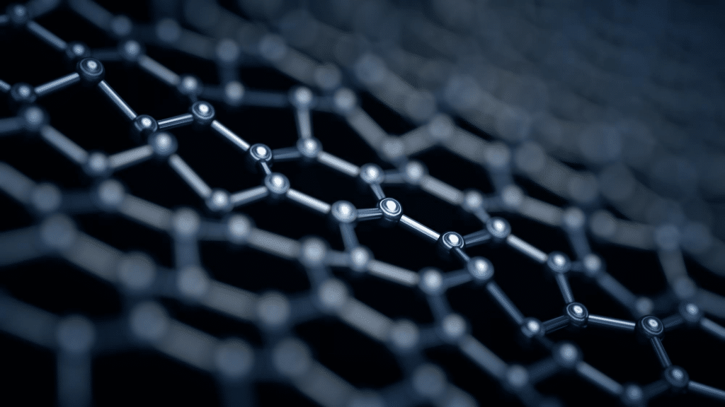
Nanoscience and technology is a new comprehensive science developed from around 1980s, it is a discipline dedicated to the study of the properties of objects with dimensional sizes ranging from 1 to 100 nm, and its creation has enabled human civilization to enter a new era - the era of nanotechnology. Nanomaterials with much smaller particles than traditional materials have many unique properties such as small size effect, quantum size effect, surface effect, interfacial effect, macroscopic quantum tunneling effect and photoelectrochemical properties. These properties make nanomaterials have many unique properties in light, magnetism, mechanics and other aspects compared with ordinary materials, thus becoming a hot spot of research in modern materials discipline.
Mechanical properties of nanofilms
Nanofilms have been widely studied for their mechanical properties far beyond those of conventional materials, especially the supermodulus and superhardness effects of thin films have become the most important research focus in the past few years. In order to fully explain these special phenomena, researchers have proposed the design theory of high-strength solids, quantum electronic effect, interfacial strain effect, and interfacial stress effect. The research on mechanical properties of nanofilms has the following three aspects: hardness, friction, toughness.
(1) hardness: mainly study the multilayer film structure in the composition ratio and modulation cycle on the hardness of the film. When the thickness of the two monolayer film in 6~8nm can be obtained when the maximum hardness of the film is about 50Gpa, which is far beyond the hardness of the single substance film. The relative ratio of the component content of the film is also an important factor affecting the hardness of the film, a two-component composition of the film, if the hard content is high, then the film hardness is high, and vice versa, it is low. Therefore, the general mechanical properties of superior film is composed of high hardness and good toughness of the components.
(2) Toughness: the improvement of toughness is proposed for the multilayer structure, the toughening mechanism is mainly crack tip passivation layer sheet pullout, crack branching, and interfacial cracking along the interface, etc., in the nano-multilayer film also exists in a similar toughening mechanism. The relative content of components in the film and the modulation wavelength are two factors that affect the toughness of the film. For example, for the metal/ceramic system, the more metal phase (toughness) content, the better the toughness of the film, but when the metal phase content exceeds a certain limit, the toughness of the film will be reduced, this phenomenon is probably due to the complex results of interfacial interaction. As for the modulation wavelength, a moderate reduction can increase the toughness of the film.
(3) Friction: the principle research for the abrasion resistance of the film is still in the exploratory stage. It has been found that a reasonable combination of components can effectively improve the wear resistance of the film. It has been found that CuNi multilayer film will greatly improve the wear resistance of 52100 bearing steel, when the modulation wavelength of the film the smaller its wear resistance is greater, this is because of the film's film interface dislocations more slip resistance. Multilayer film relative to traditional materials for the grain is smaller, longer grain boundaries, lattice defects more thus leading to slip is not easy. Moreover, there is a dislocation energy difference between the membrane layers of different materials, which makes plastic deformation more difficult.
Electrical properties of nanofilms
With the continuous development of the microelectronics industry, for the miniaturization of electronic components requirements are also increasingly high, nano-film because of its special size and performance and is widely used in electronic information interconnection technology, wiring technology, diffusion barrier layer and electronic packaging technology and so on. The electrical properties of some commonly used conductor materials (e.g., metals) change dramatically when their size is suddenly reduced to the nanometer scale. Some researchers have detected resistance anomalies in Au/AL2O3 particle films and found the following special pattern: the resistance increases linearly and sharply with the increase of Au particle content. Nanocrystalline silicon (Si) films were prepared by PECVD and found that the electrical conductivity of Si films at the nanometer scale (102 S-cm) was much higher than that in its conventional state (10″S-cm). This experiment demonstrates the relationship between the electrical conductivity of the material and the critical size of the particles: when the material particles > critical size, it will retain the conventional electrical properties, and when the material particles < critical size, it will lose the material intrinsic electrical properties.
Magnetic properties of nanofilms
Part of the thin film materials have also been widely concerned because of their special magnetic properties, and so far the phenomena of interlayer coupling, perpendicular magnetization, giant magnetoresistance effect, magneto-optical effect anomaly have been found. In the 1980s, the giant magnetoresistance effect was discovered in Fe/Cr multilayer film: the resistivity of the material itself will be changed due to the change of the magnetization state of the material. In the 1990s, this effect was observed in Co/Cu particulate films, and since then it has been found in nanosolids prepared by liquid-phase quenching and mechanical alloying. The main purpose of this effect is to reduce the saturation magnetism and to increase the sensitivity at low fields. At the present stage, two methods are probably chosen to realize it: first, thin film materials with spin-valve structure (Spin Value); second, static magnetic coupling of dipole moments between the layers by annealing the film to a certain extent so that the formation of interlayer faults. Such as Ta (100A)/Ag (20A)/[NiFe (20A)/Ag (40A)]4NiFe (20A)/Ta (40A)/Si0, (700A)/Si after 315 ℃ in the (5%H2 +95%Ar) film after annealing GMR (GradientMotionRefocussing), the film is annealed. Refocussing) reached 4%~6% magnetic field sensitivity increased. Magnetic recording materials are also a research focus of thin film materials, magnetic recording materials in order to ensure their high storage density must have good anisotropy. Relevant literature has proposed a value of K'V/kT greater than 50 (where K is the anisotropic property, V is the magnetic reversal volume, k is Boltzmann's constant, and T is the temperature). Our current research has found FePt its excellent anisotropy (about 15 times that of conventional materials).
Optical properties of nanofilms
Nanofilm materials have also gained the attention of researchers for their special properties in optics. TiO2/SnO2 superparticles and their composite LB films prepared by PCVD have special UV-Vis absorption spectra. The unique quantum effect of this composite film causes a "blue-shift" of the LB absorption spectrum, which results in good UV resistance and optical transmittance.The nanoscale particulate film composed of elements of group II-VI (CdSxSe1-x) and III-V (CaAs) undergoes optical broadening and blue-shifting during the experimental process. and blueshift. In addition, the particle films of group I-V elements (CdSSe1-) were photoinduced bleaching in the experiments, which was attributed to the change of the intensity of the absorption bands under the irradiation of certain wavelengths of light. As a new direct semiconductor material with a large bandgap (3.37 eV) and high exciton binding energy (60 meV), ZnO has become a new hot spot in the field of short-wavelength optical functional materials.
HuipingLu et al. prepared Zn0 thin films by pulsed laser deposition and investigated the effects of nitrogen and oxygen partial pressures on the microstructure, morphology and optical properties of the films. Linear and nonlinear effects of light is also a more prominent hot spot, and thin film materials because of its properties also have some value in this research. Optical linear effect: quality in the light wave field, when the light intensity is weak, the electrode of the medium is proportional to the primary side of the electric field of the light wave phenomenon. When the size of thin film materials is small enough (less than the exciton Bohr radius aB), exciton absorption peaks will appear during the experiment. For example, by controlling the film thickness of InGaAs and InGaAIAs multilayer structures, the exciton absorption peaks can be easily realized. Optical nonlinearities are the terms in the polarization intensity of a medium that are proportional to the second, third, or even higher powers of the applied electromagnetic field under the action of a strong light field. In the case of thin film materials, the quantum size effect is the main reason for optical nonlinearity. It has been found that the Z-scan curves of Ge particle films show a nonlinear enhancement of the absorption intensity of the sample along the symmetry axis of the curve where the focal point is located. Because the light intensity per unit area at the focal point is the largest, the absorption coefficient at the focal point is also the largest, with a nonlinear absorption coefficient of (β~ 0.82 cm /W), which is a third-order optical nonlinear response.
We offer Coating (micro- and nanofabrication) process customization services, Feel free to leave a message to inquire.
Related Products
Related Reading
In-depth understanding: Introduction, types and applications of electron microscope carrier mesh (copper mesh)
In-depth science: introduction, types and applications of electron microscope carrier mesh (copper mesh) Electronic display
Silicon Nitride (SiNx) Thin Films for Optical Applications
Silicon Nitride Thin Film in Optics Silicon nitride thin film as a canonical
Variation of refractive index and absorption coefficient of amorphous silicon at different wavelengths
Variation of refractive index and absorption coefficient of amorphous silicon at different wavelengths In the study of the
.jpg)