What is magnetron sputtering?

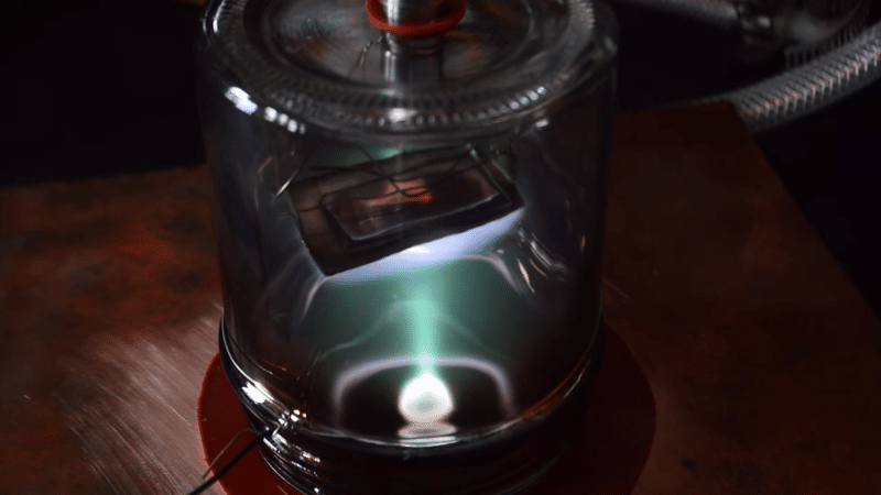
Magnetron sputtering is a commonly usedPVDThin film preparation techniques, utilizing the principles of ion bombardment and sputtering, are achieved by applying high frequency electric and static magnetic fields in a vacuum environment. In this process, the material is made in the form of a target, which is mounted inside a vacuum chamber. By applying the electric field, a plasma is formed on the surface of the target, while the static magnetic field directs the ions in the plasma to the target surface for bombardment. The bombarded target surface releases atoms or molecules which are deposited at high velocity onto the substrate surface to form a thin film.
Principle of magnetron sputtering
Sputtering coating is the process of sputtering by particle bombardment of the target material, which shoots out atoms or ions to the substrate and deposits them on the substrate to form a film layer. Magnetron sputtering is in the bipolar glow discharge when the additional magnetic field, electrons are accelerated by the electric field at the same time by the magnetic field bound, was a pendulum motion, improve the collision frequency of electrons and target particles and working gas ions, the working gas ionization degree increases, the working gas pressure is reduced, and the working gas ions are accelerated by the electric field, the impact of the target and the release of energy to the target to the target material shot target material atoms or ions, in the substrate A film layer is deposited on the surface of the substrate.
Classification of magnetron sputtering
Classification by magnetic field configuration
Planar Magnetron Sputtering (PMS)
- Conventional magnetron sputtering configuration with magnetic field parallel to the target surface.
- Suitable for uniform deposition over large areas.
Rotary Magnetron Sputtering (RMS)
- The target is rotated in a cylindrical shape to extend the life of the target.
- Ideal for deposition of films requiring large areas and high uniformity.
Dual Target Magnetron Sputtering (DMS)
- Two magnetically controlled targets are used to minimize charge accumulation on the surface of the target during the discharge process.
- Improves sputtering efficiency and film uniformity and is suitable for the preparation of electrically insulating films.
Classification by process gas
DC Magnetron Sputtering (DC Magnetron Sputtering)
- Sputtering with DC power supply, suitable for conductive targets.
- The process is simple and suitable for the deposition of thin metal films.
RF Magnetron Sputtering (RFMS)
- Sputtering with RF power supply for conductive and non-conductive targets.
- Suitable for the preparation of insulating films such as oxides and nitrides.
Classification by depositional environment
Reactive Magnetron Sputtering (RMS)
- Reaction gases (e.g., oxygen, nitrogen) are added to the argon gas, which chemically reacts with the target material to form a compound film.
- Suitable for the preparation of functional films such as oxides and nitrides.
Non-Reactive Magnetron Sputtering (NRMS)
- Deposits thin films of pure metals or alloys by sputtering using only inert gases such as argon.
- Suitable for the preparation of thin metal films.
Classification by process characteristics
Pulsed Magnetron Sputtering (PMS)
- Controlled discharge using a pulsed power supply improves sputtering stability and film quality.
- Suitable for reducing particle contamination and improving film densities.
High Power Impulse Magnetron Sputtering (HiPIMS)
- Significant improvement in sputter ionization rate and film quality using high power short pulses.
- Suitable for the preparation of high-density, low-defect films.
Classification by application area
Decorative Magnetron Sputtering (DMS)
- Used to prepare decorative coatings for surfaces such as cell phone casings, clocks, and eyeglass frames.
- Mainly using metal or alloy targets, focusing on the color and appearance of the coating.
Functional Magnetron Sputtering (FMS)
- It is used to prepare thin films with specific functions, such as optical coatings, protective coatings, and conductive films.
- Focuses on the optical, electrical, and mechanical properties of thin films.
Advantages of magnetron sputtering
- Highly controllable: precise control of film composition, structure and thickness.
- Environmentally friendly: Uses inert gases and produces less waste.
- Low temperature process: suitable for temperature sensitive substrates to avoid high temperature damage.
- High deposition rate: Enhanced plasma density for improved target sputtering efficiency.
- Low particle contamination: Reduces particulate matter generated during the reaction process and improves film purity.
- Applicable to a wide range of materials: Applicable to a wide range of targets such as metals, alloys, and compounds.
- Applicable to multilayer films: Deposition of multilayer structures or composite films is possible.
- High stability and repeatability: process stability, suitable for mass production.
- Good film uniformity and high densification: dense film with strong adhesion and uniform thickness.
Common Sputtering Materials
Aluminum (Al), Copper (Cu), Titanium (Ti), Tungsten (W), Nickel (Ni), Silver (Ag), Gold (Au), Indium Tin Oxide (ITO), Zinc Oxide (ZnO), Titanium Oxide (TiO2), Aluminum Oxide (Al2O3), Silicon Nitride (Si3N4), Titanium Nitride (TiN), Aluminum Nitride (AlN), Silicon Carbide (SiC), Titanium Carbide (TiC), Titanium / Titanium Nitride (Ti / TiN) multilayer targets, etc.. Titanium Nitride (Ti/TiN) multilayer targets, etc.
We offer Magnetron sputtering foundry customization services, Feel free to leave a message to inquire.
How to choose the right silicon nitride thin film window丨Science Guide
With this guide, you can make informed decisions to optimize your TEM imaging, SEM analysis, bioscience research, or semiconductor production.
Principles and Advantages of Plasma Enhanced Chemical Vapor Deposition (PE-CVD)
Principles and advantages of plasma enhanced chemical vapor deposition (PE-CVD)
Magnetron sputtering丨understanding the principle, classification and advantages
What is magnetron sputtering? Magnetron sputtering is a commonly used method of PVD thin film production.


.jpg)