Classification, Characterization and Applications of Physical Vapor Deposition (PVD)
Physical Vapor Deposition (PVD) is a technique used to deposit thin films on solid surfaces. It works by heating a material in a vacuum or low-pressure environment to produce vapors or ions that are deposited onto a target surface.PVD is typically used to produce thin films with specific functions or properties, such as hardness, corrosion resistance, electrical conductivity, etc.
Principle of PVD technology
PVD is a technique for depositing thin films on solid surfaces based on the process of heating a material to evaporation or sputtering temperatures, causing it to form vapors or ions, and depositing them onto a target surface.
- Vacuum environment establishment:PVD technology needs to be performed in a high vacuum or low pressure environment to ensure free propagation of material vapors or ions and to avoid collisions with gas molecules that can reduce deposition efficiency. The establishment of a vacuum environment can be realized by equipment such as vacuum pumps.
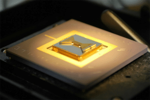
- Heating of the material:In the PVD process, the target material is heated to its evaporation temperature. The heating can be in the form of resistance heating, induction heating or electron beam heating. By heating, the surface atoms or molecules of the material are energized enough to overcome the surface tension and transform into a gaseous state.
- Evaporation or sputtering:Once the material reaches a sufficient temperature, it begins to evaporate or sputter. During evaporation, the material is directly transformed into a gaseous state, while during sputtering, energetic particles (usually noble gas ions) bombard the surface of the solid material, causing it to release atoms or molecules.
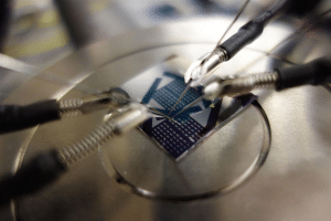
- Deposition:Material vapors or ions will be deposited onto the surface of the target substrate to form a thin film. The substrate is usually cleaned and prepared beforehand to ensure film adhesion properties and quality.
- Film formation and control:Thin films deposited on the surface of the substrate are formed gradually during the process. The thickness and nature of the film can be adjusted by controlling parameters such as deposition rate, deposition time, substrate temperature, and concentration of deposited material.
The principle of PVD technology is to use the evaporation or sputtering of materials to form thin films. By controlling the heating and deposition conditions, it is possible to achieve precise control of the thickness, composition and properties of the films to meet the needs of different applications.
Classification of PVD technology
Principle: Controlled ion bombardment of a solid target using a magnetic field to generate energetic ions and release them onto the target surface.
Features: Typically higher deposition rates and more uniform film thickness distribution.
Applications: Widely used in the preparation of semiconductor devices, optical films, etc.
Electron Beam Evaporation (EBE)
Principle: Using an electron beam to heat the material to vaporize it to form a thin film.
Features: Higher deposition rate and higher deposition temperature, suitable for deposition of high melting point materials.
Application: Mainly used for the preparation of metal films or coatings of other high melting point materials.
Laser Ablation
Principle: A laser is used to heat the material, causing it to vaporize and deposit onto the substrate surface.
Characteristics: Localized deposition of specific areas can be achieved, applicable to the field of micro and nano processing.
Applications: Mainly used for the preparation of functional coatings, nanostructures, etc.
Thermal Evaporation (Thermal Evaporation)
Principle: PVD technology based on heating the material to its evaporation temperature to form a vapor.
Characteristics: Used for the preparation of metal films or other low melting point materials for deposition.
Application: Mainly used for the preparation of metal coating, optical thin film, etc.
Each technology has its own unique principles, characteristics and areas of application. Choosing the right PVD technology depends on the specific application requirements, material properties, and desired film performance.
Advantages of PVD
- High purity and quality films: Deposited in a high vacuum environment to reduce impurities and contamination and ensure film purity.
- Good film uniformity: obtaining films with good uniformity and consistent thickness by precisely controlling the process parameters.
- High adhesion and densification: Ion plating and sputtering technologies can enhance the adhesion and densification of thin films.
- wide application: Capable of handling a wide range of materials, including metals, alloys, oxides, nitrides and carbides, with a high degree of adaptability.
- environmental: PVD technology uses fewer chemicals and is more environmentally friendly than chemical deposition processes.
PVD Applications
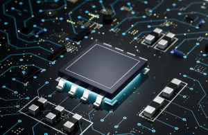
Electronics and semiconductor industry
- metal interconnect layer: Used for metallic interconnect layers such as aluminum and copper in integrated circuits to provide conductive paths.
- Barrier and diffusion layersAsTitanium Nitride (TiN)Used to block diffusion of metal atoms and improve device stability.
- Film Resistors and Capacitors: For the manufacture of precision thin film resistors and capacitors.
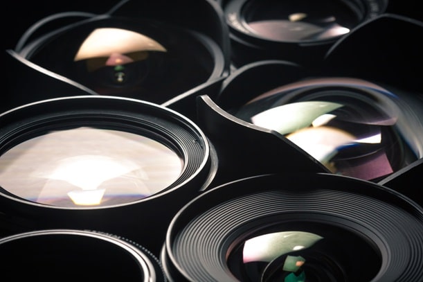
Photonics and optics industry
- Anti-Reflective Coating: Anti-reflective coatings for eyeglasses, cameras and solar cells to improve light transmission.
- reflective coating: For highly reflective coatings in mirrors, lasers and optical instruments.
- optical filter: Filters for optical communication and optical sensors, regulating light wavelength and transmittance.
Machinery and tools industry
- Wear-resistant coatingAsTitanium Nitride (TiN)The coating of titanium carbide (TiC) and diamond-like carbon (DLC) is used on cutting tools, molds and mechanical parts to improve wear resistance and service life.
- Anti-corrosion coating: For anti-corrosion coatings in chemical equipment and marine environments to extend service life.
Decorative Coating
- Decorative coatings: Decorative coating for clocks, jewelry, cell phone cases and eyeglass frames, providing an attractive appearance and wear resistance.
biomedical
- Biocompatible coatings: Biocompatible coatings such as titanium and titanium nitride for medical devices and implants to improve biocompatibility and corrosion resistance.
- Drug delivery systems: For the fabrication of nanoscale drug delivery vehicles for controlled release and targeted delivery of drugs.
Energy and environment
- solar cell: For the deposition of transparent conductive films, buffer and absorber layers to improve photovoltaic conversion efficiency.
- Fuel cells and batteries: Used in the preparation of high-performance electrode materials, such as silicon-based anodes in lithium-ion batteries and lithium iron phosphate (LiFePO4) anode materials.
PVD technology plays an important role in improving the surface properties of materials, adding new functions, and improving product quality and performance. With the continuous development of science and technology, the application fields of PVD technology will continue to expand and deepen.
We offer Physical Vapor Deposition (PVD) OEM Customization Services, Feel free to leave a message to inquire.
Related Products
Related Reading
Chemical Vapor Deposition (CVD) Classification, Characteristics, and Applications
Chemical Vapor Deposition (CVD) Classification, Characteristics, and Applications Chemical Vapor
What are the properties and applications of electron beam evaporation plated silica films?
What are the properties and applications of silicon dioxide films prepared by electron beam evaporation? Dioxide
Influence of the annealing process on the platinum resistance
Influence of the annealing process on platinum resistors In the field of high-precision temperature measurement, thin-film
.jpg)