What is the thin film deposition process ?
As an important material preparation method, thin film deposition technology is widely used in electronic device manufacturing, optical coating, new energy field and functional thin film and many other fields. The development of thin film deposition technology not only promotes the progress of materials science and engineering technology, but also provides strong support for the sustainable development of human society.
Principles of thin film deposition technology
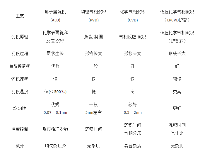
Thin film deposition technology is the process of depositing thin films on solid surfaces by physical or chemical means. Common thin film deposition methods include physical vapor deposition (PVD), chemical vapor deposition (CVD), solution methods, and atomic layer deposition (ALD).
In the PVD process, the material is vaporized and deposited on the substrate surface by thermal evaporation or sputtering, etc., while CVD generates a solid product on the surface by a chemical reaction in the gas phase. The solution method is used to form a thin film by causing a solute in solution to be deposited on the surface of the substrate, while ALD prepares thin films by layer-by-layer deposition with excellent film uniformity and control.
Comparison of Thin Film Deposition Processes
Application of thin film deposition technology
electronic equipment manufacturing
Transistor manufacturing: In transistor manufacturing, thin film deposition techniques are used to prepare functional films such as insulating layers and metal conductors. For example, silica insulating layers are prepared using physical vapor deposition (PVD) or chemical vapor deposition (CVD) to optimize the insulating properties of transistors.
Integrated Circuit (IC) Manufacturing: In the IC manufacturing process, metal layers, multilayer metal layers, etc. are prepared by thin film deposition techniques for connection and wiring. For example, aluminum films are deposited by PVD for metal line preparation, and multilayer silicon oxide is prepared by CVD for insulating layer preparation.
Flat panel display manufacturing: in the liquid crystal display and OLED manufacturing process, the use of thin film deposition technology to prepare transparent conductive film, organic light-emitting layer, etc.. Such as the use of evaporation method for ITO conductive film preparation, in order to realize the display of light transmission and conductive function.
Optical
Lens Coating: In optical lens preparation, thin film deposition technology is used to prepare anti-reflective films and reflective films. Multi-layer dielectric reflective films are prepared by sputtering method, which can improve the transmittance and reflectivity of the lens.
Filter Preparation: Optical filters are usually prepared by thin film deposition techniques with specific wavelength transmission characteristics. For example, CVD is used to prepare optical filters with a multilayer film stack structure to achieve selective transmission and reflection of light at specific wavelengths.
New Energy Sector
Thin-film solar cells: Thin films of amorphous silicon, copper indium gallium selenide (CIGS) and other materials are prepared by thin-film deposition technology for the preparation of thin-film solar cells. These thin-film solar cells are characterized by high conversion efficiency, thinness and flexibility.
Fuel cell membrane layer: In fuel cells, thin films such as titanium oxides and yttrium oxide stabilized oxides are prepared by atomic layer deposition (ALD) and other techniques as proton transport layers and hydrogen barrier layers to improve the performance and stability of fuel cells.
Functional Film Field
ITO conductive film: Indium Tin Oxide (ITO) film as a transparent conductive film has important applications in the field of touch screen and liquid crystal display. ITO film is prepared by sputtering method to realize current transmission and light transmission.
Magnetic films: In the preparation of devices such as magnetic heads for hard disks, magnetic films are prepared using techniques such as sputtering or evaporation to achieve high sensitivity and stability in data reading and writing.
Medical devices and biomedical field
Biosensors: In the biomedical field, thin-film deposition techniques are used to prepare functional films required for biosensors. For example, atomic layer deposition techniques are utilized to prepare thin films of specific materials for sensitive detection and analysis of biosensors.
Drug release systems: nanofilms containing drugs are prepared by thin film deposition techniques and are used to control the rate and location of drug release for targeted therapy and medical treatment.
Environmental protection and energy conservation
Photocatalytic materials: Photocatalytic materials, such as titanium dioxide films, are prepared using thin-film deposition technology for degrading pollutants and purifying water. These films have efficient photocatalytic properties and have important applications in environmental protection.
Heat Transfer Thin Films: Thin films of materials with excellent heat transfer properties are prepared by thin film deposition technology for use in the preparation of energy-saving materials and equipment to improve energy utilization efficiency.
Materials Science and Surface Engineering
Anti-corrosion coatings: Thin film deposition technology is utilized to prepare thin films of materials with corrosion resistance for use in aerospace, automotive manufacturing and other industries to extend the life of the material and improve durability.
Nanostructured materials: Thin films of materials with specific nanostructures, such as nanowires and nanoparticles, are prepared by thin-film deposition techniques for the study of material properties and the development of new materials.
Nanotechnology and micro-nanofabrication
Nanostructured thin films: Thin film deposition techniques are widely used in the field of nanotechnology to prepare thin film materials with nanostructures. These nanostructured thin films have important applications in the field of nanodevices, nanosensors, etc., such as the preparation of thin films of gold nanoparticles for surface-enhanced Raman spectroscopy (SERS) by sputtering.
Templates for micro- and nanofabrication: Thin film deposition techniques are used to prepare micrometer-scale templates for micro- and nanofabrication and nano-printing. High-quality metal films are prepared by CVD or PVD and used as etch masks or deposition templates for micro- and nanofabrication.
Aerospace and Defense
High-temperature protective coatings: In the aerospace field, thin-film deposition techniques are used to prepare high-temperature protective coatings to improve the heat resistance and protective properties of aircraft. For example, silicon carbide films are prepared using CVD technology for high-temperature protection of missile engines.
Coatings for radar and optoelectronic sensors: Coatings with specific optical properties are prepared by thin-film deposition technology and are used to improve the stealth and detection performance of radar, infrared sensors and other equipment.
Construction materials and coatings
Architectural Glass Coatings: Utilizing thin film deposition technology to prepare solar control coatings for thermal and light insulation of architectural glass to improve building energy efficiency performance.
Anti-fouling coatings: Anti-fouling coatings, such as super-hydrophobic surface coatings or antimicrobial coatings, are prepared by thin-film deposition techniques and applied to the surfaces of building materials and facilities to reduce contamination and maintenance costs.
We offer Coating (micro- and nanofabrication) process customization services, Feel free to leave a message to inquire.
Related Products
Related Reading
Physical Vapor Deposition (PVD) Classification, Characteristics, and Applications
Classification, Characteristics, and Applications of Physical Vapor Deposition (PVD) Physical Vapor
Principles and Advantages of Plasma Enhanced Chemical Vapor Deposition (PE-CVD)
Principles and advantages of plasma enhanced chemical vapor deposition (PE-CVD)
What are the properties and applications of electron beam evaporation plated silica films?
What are the properties and applications of silicon dioxide films prepared by electron beam evaporation? Dioxide
.jpg)