PECVD vs. magnetron sputtering: which technique is better for preparing amorphous silicon thin films?
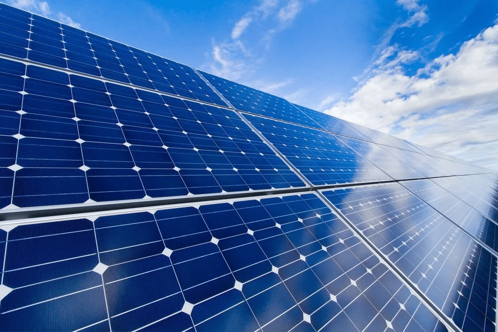
Silicon thin film solar cell research is the international photovoltaic field research hotspot, silicon thin film solar cells relative to monocrystalline silicon and polycrystalline silicon solar cells, with fewer consumables, low cost characteristics. Amorphous silicon thin film solar cell production process is simple, low substrate temperature, easy to apply the integration process and large-area production, it is the most promising class of silicon thin film solar cells. In the process of preparing amorphous silicon thin-filmPlasma Enhanced Chemical Vapor Deposition (PECVD)andmagnetron sputteringare two widely used techniques. Each technique has its unique advantages and limitations for different application scenarios.
Advantages and Applications of PECVD
PECVD technology generates a plasma by using RF or microwave energy to excite a silicon-containing gas (usually silane SiH₄), which in turn deposits an amorphous silicon thin film on a substrate at a lower temperature (about 200°C to 300°C). The main advantage of this technique is:
- Low-temperature processes: For temperature-sensitive substrates such as plastics or certain biological materials.
- High-quality membrane layer: The hydrogen content in the membrane can be adjusted, which helps to minimize microscopic defects within the membrane and improves the electrical properties of the membrane.
- Uniform large-area coating: suitable for mass production, especially in areas such as solar cells and flat panel displays.
PECVD equipment is relatively complex and costly, and the production rate is limited by the chemical reaction rate. During the preparation process, a large amount of gas is discharged directly out of the equipment without reaction, and gas utilization is low. Because the method is ionized gas, there is a high air pressure in the reaction chamber, which will hinder the deposition of particles, and in order to ensure the quality of film formation, and can not use too high a power, so the film deposition rate will be slow.
Advantages and applications of magnetron sputtering
Magnetron sputtering controls the plasma by creating a magnetic field, which allows the sputtered particles to be deposited onto the substrate more efficiently. The main advantages of this technique include:
- Suitable for a wide range of materials: Conductive and non-conductive materials can be processed, by selecting different targets and substrates.
- Simple and less expensive equipment: Compared to PECVD, magnetron sputtering equipment is usually simpler and cheaper, with lower maintenance costs.
- High deposition rate: high productivity, especially suited for industrial applications requiring rapid production of large quantities.
While the preparation of amorphous silicon films by magnetron sputtering offers advantages such as high deposition rates and relatively low equipment costs, it also faces a number of challenges, including possible defects in film quality, difficult-to-control hydrogen content, more complex equipment maintenance requirements, potential risk of damage to the substrate, and higher energy consumption, and the quality of the film layers may not be as good as those prepared by PECVD.
Process Comparison
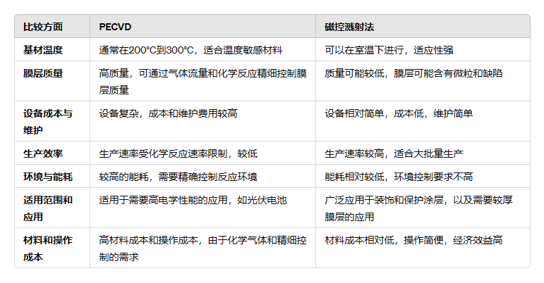
Comprehensive comparison and selection
The choice of technology depends largely on the needs of the end product and cost-benefit considerations. If your application requires high quality, electrically sound amorphous silicon films and the substrate is temperature sensitive, PECVD may be the more appropriate choice. However, if cost is an important factor, or if the product needs are such that a slightly lower film quality is acceptable, magnetron sputtering may be a more cost-effective option.
Factors such as equipment availability, technical support, and experience also need to be considered in the actual selection process. In-depth conversations with our industry experts and engineers can help you make a more informed decision.
We offer Coating (micro- and nanofabrication) process customization services, Feel free to leave a message to inquire.
Physical Vapor Deposition (PVD) Classification, Characteristics, and Applications
Classification, Characteristics, and Applications of Physical Vapor Deposition (PVD) Physical Vapor
What is thin film deposition process
What is thin film deposition ? Thin film deposition technology is an important
Variation of refractive index and absorption coefficient of amorphous silicon at different wavelengths
Variation of refractive index and absorption coefficient of amorphous silicon at different wavelengths In the study of the

.jpg)