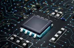
Principle and characteristics of thin film preparation by sputtering method
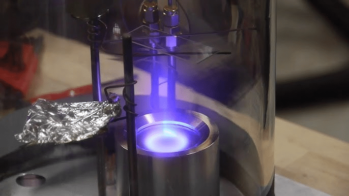
Sputtering technology isPhysical vapor deposition (PVD)A kind of, can be used for the preparation of insulators, metals and other thin films, composite films can also be prepared, the theory can be sputtered almost all enough to make a solid target metals, alloys, polymer compounds and ceramic materials, etc., the preparation of thin films, fast, low-temperature, small damage to the film; preparation of thin films prepared by the film layer uniformity, no internal air holes, high density, good adhesion with the substrate, high film quality.Magnetron sputtering technologyThe proposed sputtering rate and target utilization have been greatly improved, and have been widely used in scientific research and industrial production.
gas glow discharge
Sputtering process is built on the basis of gas glow discharge, glow discharge is a type of gas discharge, is a kind of ion bombardment of the cathode to produce secondary electrons to maintain a stable self-sustained discharge due to the sputtering chamber still exists in a small number of ions and electrons, so just add the negative voltage, not yet produced glow discharge, the current at this time is small, the current is almost unchanged, to participate in the movement of the number of charges determine the The current strength, at this time called for the dark light discharge. When the voltage continues to increase, the sputtering chamber in the energy of electrons and charged ions gradually increased, in the electric field for accelerated motion of electrons and charged ions continue to collide with the electrodes and electrified gas atoms, charged particles continue to increase, the current increases. Afterwards, with the increase in the number of charged particles, the current is also slowly rising, the voltage remains unchanged, this discharge region is called "Thomson discharge zone". Finally, the development of "avalanche", positive away from the cathode target surface continued bombardment, there are constantly secondary electrons are bombarded out, the release of secondary electrons and sputtering chamber in the gas collision, the formation of more positive ions, positive ions followed by bombardment of the target produced by the secondary electrons, and then with the gas atoms collide to form more positive ions. In this process, when the discharge process of the system reaches self-sustained, the gas begins to glow, the voltage decreases, and then the current suddenly rises, usually called a region of "normal discharge zone". Afterwards, the power is increased and the current and voltage density between the two electrodes increases, at which time the glow discharge stabilizes, and this region is called the "abnormal glow discharge region", which is the region actually used in sputtering technology. This is followed by the "arc discharge zone", which is the area where the voltage between the poles drops to a very low level after the abnormal glow discharge zone.
DC magnetron sputtering
In a low voltage DC glow discharge, the process is divided into five zones: the cathode zone, the negative glow zone, the Faraday dark zone, the positive column zone and the anode zone. One of these zones, the anomalous glow discharge, is the one actually used for sputtering the deposited film. In sputtering the substrate acts as the anode, usually placed in the negative glow region, and the target acts as the cathode. Since the energy and velocity of electrons are much higher than those of ions, a plasma sheath layer is formed during the glow discharge and, due to the presence of the sheath potential, a large portion of the applied voltage at the electrode is taken up by the cathode sheath potential. The establishment of the plasma sheath potential causes the ions reaching the cathode to be accelerated accordingly and gain energy. Therefore, the ions have high energy when they reach the surface of the cathode through the plasma region of the glow discharge, and produce a bombardment effect on the surface of the cathode, so that the molecules and atoms of the cathode material are sputtered out and the sputtering phenomenon occurs. These molecules and atoms have a certain amount of kinetic energy and are shot in a certain direction toward the surface of the workpiece to form a thin film.
Sputtering is a complex process in which sputtering is accompanied by various phenomena of ion bombardment. The basic condition for thin film deposition is that most of the particles ejected from the solid surface under the high-speed collision of incident particles are neutral atoms or molecules. In addition to this, the radiated secondary electrons are the elementary particles that maintain the glow discharge in sputtering, and their energy is equal to the potential of the target.
Diode sputtering is the earliest sputtering method to realize technical application. The sputtering device of diode sputtering consists of two electrodes, the cathode and the anode, so it is also called cathodic sputtering or direct current (DC) sputtering.
Due to the existence of dipolar sputtering gas ionization rate is low (in 0.3 % ~ 0.5%), the deposition rate is slow, the target material utilization rate is low, the electrons make the substrate temperature rise and other shortcomings, so the sputtering technology was not widely used, in order to make up for these shortcomings, in the last century, 1970's put forward the magnetron sputtering technology. Magnetron sputtering technology attenuates the damage to the film caused by the heat of secondary electrons hitting the substrate and improves the sputtering rate of dipolar sputtering. Therefore, magnetron sputtering technology has gained rapid development and wide application as soon as it was introduced, and now it has become one of the mainstream technologies for material surface coating.
The magnet is placed at the back of the target, so that the surface of the magnetic line of force that penetrates out of the target forms a structure that is perpendicular to the electric field and eventually returns to the target surface. The binding effect of the magnetic field on the secondary electrons on the target surface significantly increases the plasma concentration near the target surface, thus effectively solving the problem of low deposition rate of ordinary dipole sputtering. Electrons in the electric and magnetic fields, the trajectory is bent, in the process of flying to the substrate electrons and gas atoms collision, so that the gas molecules ionized cations and electrons, electrons to the anode, and cations will be accelerated under the action of the electric field to the target, and high energy bombardment of the target surface, so that the target material sputtering, sputtering out of the neutral target atoms (or molecules) in the substrate deposition of the film formation.
reactive sputtering
If the film to be prepared is a compound, there are two methods, (1) direct sputtering of the target material of the compound, and (2) it can be prepared by reactive sputtering. Since the molecules of the former compound, after being sputtered, may decompose in a plasma atmosphere due to the impact of electrons, and the final thin film obtained does not have the same chemical composition as the target material substance, thin films are sometimes prepared by reactive sputtering. Reactive sputtering is usually used to sputter compound films such as oxides or nitrides (tantalum nitride, silicon nitride, superconducting films, ITO transparent conductive films, etc.). During the experiment, an appropriate amount of reactive gas (e.g. nitrogen, oxygen, etc.) is mixed into the sputtering gas, and the nitrogen or oxygen will be transformed into negative ions in the sputtering chamber, which will react with the bombarded atoms or atom groups of the target material to form compounds. The advantage of reactive sputtering is that the chemical composition of the film can be controlled by adjusting the process parameters at the time of sputtering, adjusting the components of the film and realizing the purpose of precisely controlling the film components. According to the deposition rate of reaction sputtering can be divided into three categories: transition mode, metal mode, oxide mode.
RF sputtering
Radiofrequency (RF) sputtering, also known as high-frequency sputtering, was invented for sputtering insulating material materials. Diode sputtering and magnetron sputtering can sputter metals and semiconductors, but not insulators. This is due to the fact that ions impinge on an insulator target and then charge the target, and when the potential of the target rises, the ion accelerating field becomes smaller until sputtering stops and the glow discharge stops, resulting in the sputtering not continuing. This is the reason why diode sputtering and magnetron sputtering can only sputter conductors and semiconductors, but not thin films of insulators, thus leading to the development of RF sputtering.
The principle of radio frequency sputtering is that if a radio frequency voltage is applied to the target, when a sinusoidal wave is applied to the target in the positive half-cycle, because the mass of electrons is smaller than the mass of ions, the electrons are easier to move than the positive ions, the mobility is higher, and therefore the electrons are able to fly to the target in a very short period of time to neutralize the positive charges accumulated on the surface of the target and deposit a large number of electrons on the surface of the target, so that the target shows a negative potential and attracts positive ions to Continue to bombard the target surface sputtering, so that the positive and negative half-cycle, sputtering phenomenon continues to produce. High-frequency alternating current (HFAC) electric field makes the target material alternately bombarded by ions and electrons, and the shock of electrons in the high-frequency electric field increases the ionization probability, thus the sputtering rate of RF sputtering is higher than that of dipole sputtering. RF sputtering can not only sputter insulators, conductors can also be sputtered by RF sputtering.
In addition to the above sputtering methods, there are also ion sputtering, bias sputtering, ECR sputtering and others.
We offer Sputtering Foundry Customization Services, Feel free to leave a message to inquire.
Related Products
Related Reading
Introduction of 3 applications of silicon nitride thin film windows in materials science
3 Application Scenarios of Silicon Nitride Thin Film Windows in Materials Science Silicon Nitride Thin
What are the characteristics and applications of vanadium dioxide prepared by magnetron sputtering
What are the characteristics and applications of vanadium dioxide prepared by magnetron sputtering Magnetron sputtering method
What are the factors that influence the sputter coating process on thin film materials?
What are the factors that influence the sputtering coating process on thin film materials? With high energy
.jpg)