Difference between LPCVD and PECVD
Difference between LPCVD and PECVD By operating at high temperatures in a low-pressure environment, L
Home " Product " Nano-embossed stencil " Nanoimprint Stencil丨Wire Grid Array Grid Nano Stencil - Harbor Semiconductor
| Periodicity | Effective area | Maximum etching depth (silicon/quartz) | Line Width | Model |
| 125nm | φ 80 mm | 100 nm/80 nm | 50~80 nm | L125_D80 |
| 140nm | φ 80 mm | 100 nm/80 nm | 50~85 nm | L140_D80 |
| 150nm | φ 90 mm | 75 nm/80 nm | 60~100 nm | L150_D90 |
| 200nm | φ 90 mm | 150 nm/120 nm | 60~120 nm | L200_D90 |
| 250nm | φ 94 mm | 200 nm/100 nm | 90~130 nm | L250_D100 |
| 280nm | φ 80 mm | 200 nm/100 nm | 100~150 nm | L280_D80 |
| 300nm | φ 94 mm | 300 nm/100 nm | 100~160 nm | L300_D100 |
| 380nm | φ 94 mm | 400 nm/300 nm | 200~270 nm | L380_D100 |
| 400nm | φ 94 mm | 300 nm/150 nm | 100~200 nm | L400_D100 |
| 470nm | φ 94 mm | 500 nm/400 nm | 200~270 nm | L470_D100 |
| 500nm | φ 94 mm | 400 nm/200 nm | 150~250 nm | L500_D100 |
| 560nm | φ 80 mm | 400 nm/200 nm | 150~280 nm | L560_D80 |
| 600nm | φ 94 mm | 500 nm/250 nm | 150~300 nm | L600_D100 |
| 760nm | φ 94 mm | 700 nm/600 nm | 320~430 nm | L760_D100 |
| 800nm | φ 94 mm | 600 nm/300 nm | 200~400 nm | L800_D100 |
| 1000nm | φ 94 mm | 800 nm/400 nm | 200~500 nm | L1000_D100 |
| 1300nm | 75x55 mm² | 1000 nm/500 nm | 300~650 nm | L1300_75x55 |
| Periodicity | Effective area | Maximum etching depth (silicon) | Line Width | Model |
| 125nm | 18x18 mm² | 120 nm | 60 nm | L125_18x18 |
| 150nm | 15x15 mm² | 150 nm | 75 nm | L150_15x15 |
| 200nm | 20x20 mm² | 60 nm/90 nm | 100 nm | L200_20x20 |
| 300nm | 30x30 mm² | 170 nm | 170 nm | L300_30x30 |
| 375nm | 20x20 mm² | 264 nm | 240 nm | L375_20x20 |
| 550nm | 20x20 mm² | 300 nm | 288 nm | L550_20x20 |
| 600nm | 20x20 mm² | 100 nm | 400 nm | L600_20x20 |
| 800nm | 20x20 mm² | 380 nm | 400 nm | L800_20x20 |
| 1300nm | φ 50 mm | 480 nm | 750 nm | L1300_D50 |
| 4000nm | 32x32 mm² | 2000 nm/2300 nm | 2000 nm | L4000_32x32 |
| 4800nm | 25x25 mm² | 2600 nm/3200 nm | 2200 nm | L4800_25x25 |
| Periodicity | Effective area | Maximum etching depth | Line Width | Model |
| 10μm | 20x20 mm² | 5 μm (silicon) | 400 nm | VL10_20x20 |
| 80 μm | φ 100 mm | 7.5 μm (Nickel) | 4 μm | VL80_D100 |
Features and Benefits:
High resolution: Our nanoimprint stencil has excellent resolution capabilities, allowing for complex patterning at the nanoscale. This high-resolution property makes it ideal for studying nanoscale phenomena and fabricating nanodevices.
High precision: Our stencil manufacturing process uses advanced nanofabrication technology to ensure a high degree of consistency and precision. This high precision ensures that each stencil provides reliable and repeatable pattern transfer results.
Versatility: Our nanoimprint stencil can be used for a variety of applications. It can be used to fabricate nanoelectronic devices, such as nanotransistors and nanowires. It can also be used for the fabrication of optoelectronic devices, such as nano gratings and photonic crystals. In addition, it has a wide range of applications in the biomedical field, such as the fabrication of biochips and nanosensors.
Efficient: Our nanoimprint stencil manufacturing process is efficient and scalable. It can be mass-produced for large-scale manufacturing needs. This high efficiency makes our products the first choice for industrial and academic research.
Customization: We can provide customized nano-embossing stencils according to the needs of our customers. Whether it's a specific pattern design or a special material requirement, our team can tailor the best solution for you.
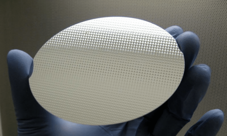
A nanoimprinting template (wire grid array) is a key component used in nanoimprinting technology. It is a template consisting of nanoscale wire grid patterns used to achieve high-resolution pattern transfer on the surface of the target material.
The main feature of nanoimprinted stencils (wire grid arrays) is their wire grid structure. A wire grid is a pattern of long, thin strips arranged in parallel. The spacing and size of these grids can be precisely controlled on the nanoscale, typically between a few tens and a few hundred nanometers. The shape and arrangement of the grids can be designed and customized to meet specific application requirements.
Product accuracy:
Height/Depth: ± 15% Line Width: ± 10%
Diameter: ± 10% Defect area: < 1%

Difference between LPCVD and PECVD By operating at high temperatures in a low-pressure environment, L

Principles and Applications of Optical Coating Technology The process principles of optical coating are mainly involved in the optical element
Influence of the annealing process on platinum resistors In the field of high-precision temperature measurement, thin-film-type platinum resistors are used because of
Magnetron sputtering丨the process of making platinum temperature sensors In modern technology, temperature sensors
.jpg)